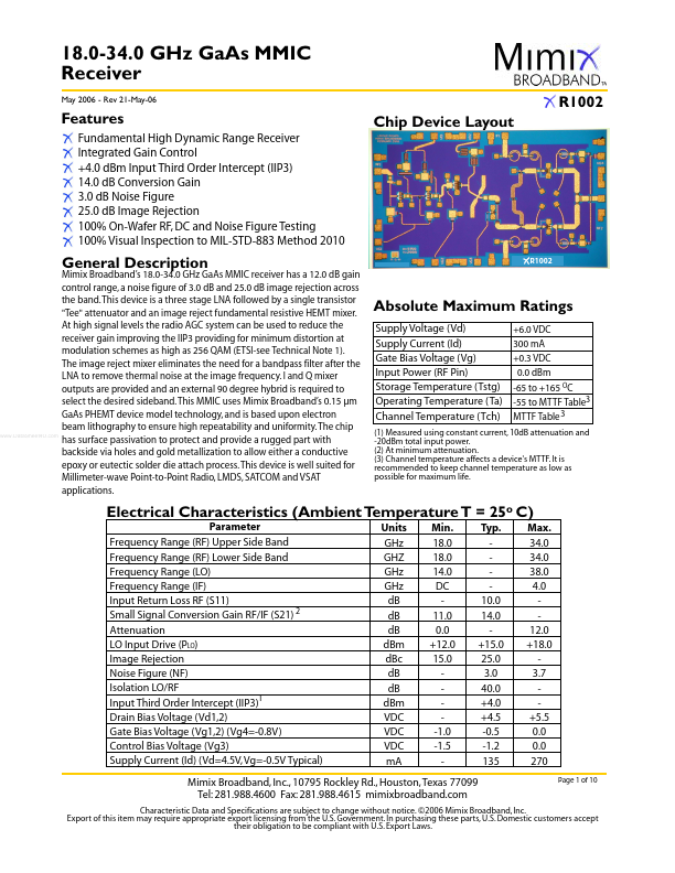
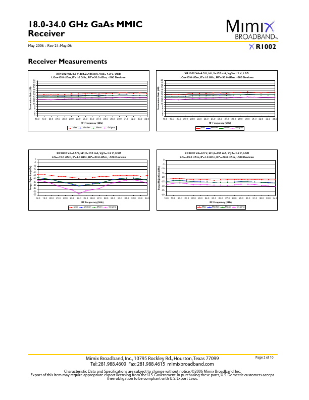
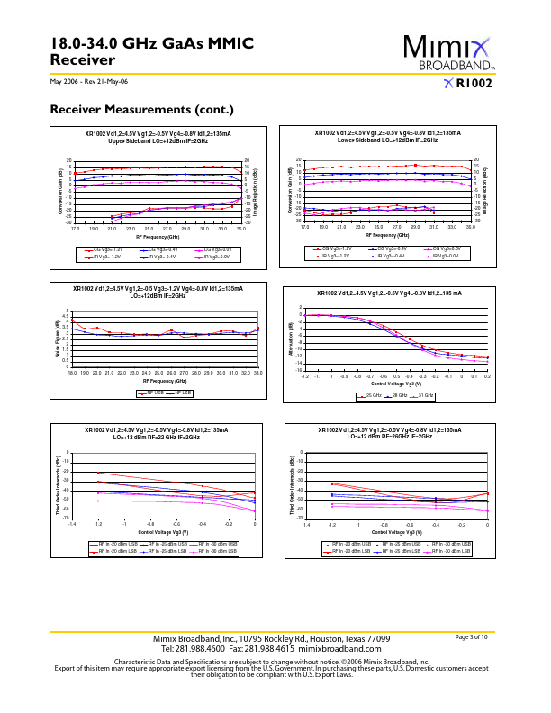
Datasheet4U Logo Datasheet4U.com

XR1002 - GaAs MMIC Receiver

Description

R1002 Absolute Maximum Ratings Supply Voltage (Vd) Supply Current (Id) Gate Bias Voltage (Vg) Input Power (RF Pin) Storage Temperature (Tstg) Operating Temperature (Ta) Channel Temperature (Tch) +6.0 VDC 300 mA +0.3 VDC 0.0 dBm -65 to +165 OC -55 to MTTF Table3 MTTF Table 3 www.DataSheet4U.com (

Features

  • Fundamental High Dynamic Range Receiver Integrated Gain Control +4.0 dBm Input Third Order Intercept (IIP3) 14.0 dB Conversion Gain 3.0 dB Noise Figure 25.0 dB Image Rejection 100% On-Wafer RF, DC and Noise Figure Testing 100% Visual Inspection to MIL-STD-883 Method 2010 Mimix Broadband’s 18.0-34.0 GHz GaAs MMIC receiver has a 12.0 dB gain control range, a noise figure of 3.0 dB and 25.0 dB image rejection across the band. This device is a three stage LNA followed by a single transistor "Tee" at.

📥 Download Datasheet

Datasheet preview – XR1002

Datasheet Details

Part number XR1002
Manufacturer Mimix Broadband
File Size 428.12 KB
Description GaAs MMIC Receiver
Datasheet download datasheet XR1002 Datasheet
Additional preview pages of the XR1002 datasheet.
Other Datasheets by Mimix Broadband

Full PDF Text Transcription

Click to expand full text
18.0-34.0 GHz GaAs MMIC Receiver May 2006 - Rev 21-May-06 Features Fundamental High Dynamic Range Receiver Integrated Gain Control +4.0 dBm Input Third Order Intercept (IIP3) 14.0 dB Conversion Gain 3.0 dB Noise Figure 25.0 dB Image Rejection 100% On-Wafer RF, DC and Noise Figure Testing 100% Visual Inspection to MIL-STD-883 Method 2010 Mimix Broadband’s 18.0-34.0 GHz GaAs MMIC receiver has a 12.0 dB gain control range, a noise figure of 3.0 dB and 25.0 dB image rejection across the band. This device is a three stage LNA followed by a single transistor "Tee" attenuator and an image reject fundamental resistive HEMT mixer.
Published: |