Datasheet4U Logo Datasheet4U.com

MCM63F919 - 256K x 36 and 512K x 18 Bit Flow-Through BurstRAM Synchronous Fast Static RAM

Download the MCM63F919 datasheet PDF. This datasheet also covers the MCM63F837 variant, as both devices belong to the same 256k x 36 and 512k x 18 bit flow-through burstram synchronous fast static ram family and are provided as variant models within a single manufacturer datasheet.

General Description

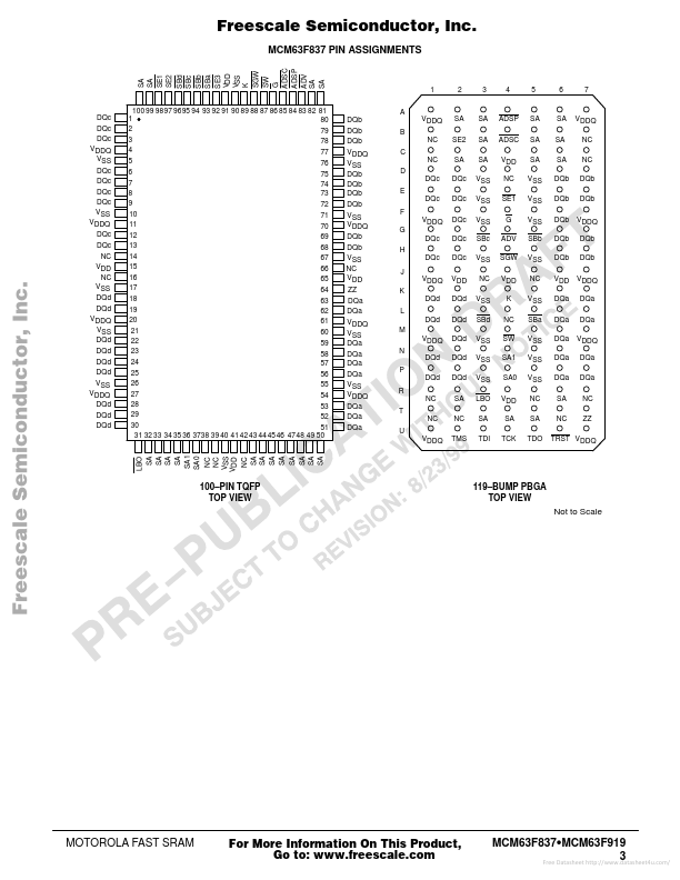
Pin Locations 85 Symbol ADSC Type Input Description Synchronous Address Status Controller: Active low, interrupts any ongoing burst and latches a new external address.

Used to initiate a READ, WRITE, or chip deselect.

Key Features

  • ables output buffers (DQx pins). High.
  • DQx pins are high impedance. Clock: This signal registers the address, data in, and all control signals except G, LBO, and ZZ. Linear Burst Order Input: This pin must remain in steady state (this signal not regist.

📥 Download Datasheet

Note: The manufacturer provides a single datasheet file (MCM63F837_Motorola.pdf) that lists specifications for multiple related part numbers.

Full PDF Text Transcription (Reference)

The following content is an automatically extracted verbatim text from the original manufacturer datasheet and is provided for reference purposes only.

View original datasheet text
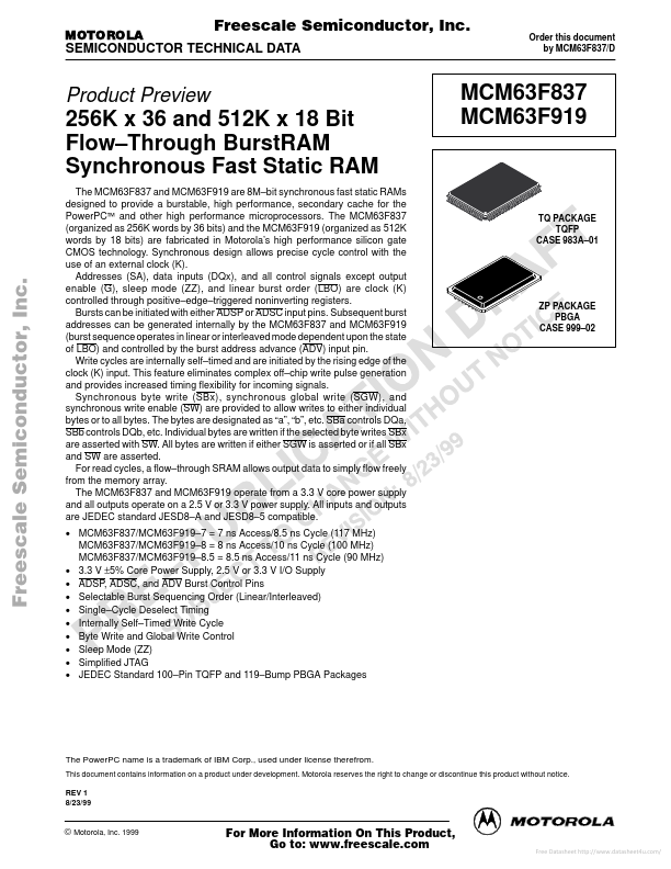
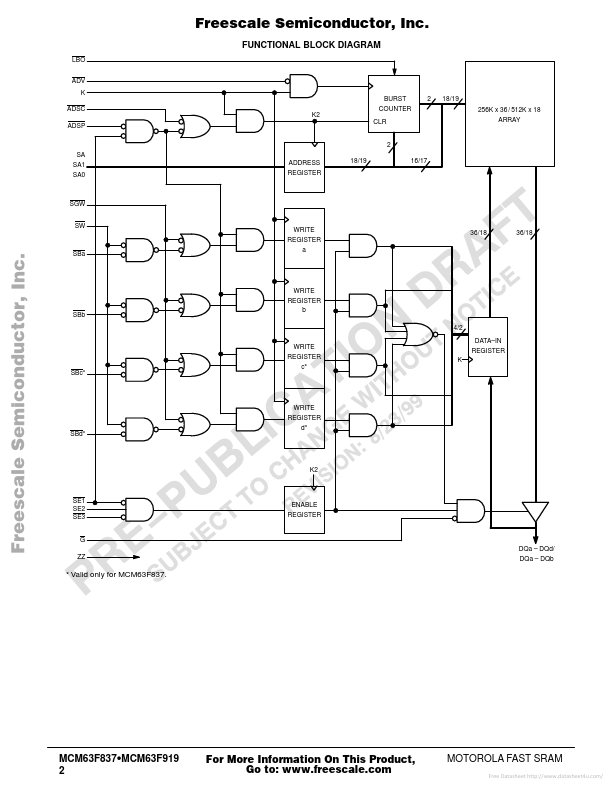
MOTOROLA Freescale Semiconductor, Inc. SEMICONDUCTOR TECHNICAL DATA Order this document by MCM63F837/D Product Preview 256K x 36 and 512K x 18 Bit Flow–Through BurstRAM Synchronous Fast Static RAM The MCM63F837 and MCM63F919 are 8M–bit synchronous fast static RAMs designed to provide a burstable, high performance, secondary cache for the PowerPC™ and other high performance microprocessors. The MCM63F837 (organized as 256K words by 36 bits) and the MCM63F919 (organized as 512K words by 18 bits) are fabricated in Motorola’s high performance silicon gate CMOS technology. Synchronous design allows precise cycle control with the use of an external clock (K).