rd mounted components. Most power electronic loads are inductive; the data in the figure is taken with a resistive load, which approximates an optimally snubbed inductive load. Power MOSFETs may be safely operated into an inductive load; however, snubbing reduces switching losses. 15000 Ciss
VDS = 0 V
VGS = 0 V
TJ = 25°C
12000 C,.
The following content is an automatically extracted verbatim text
from the original manufacturer datasheet and is provided for reference purposes only.
View original datasheet text
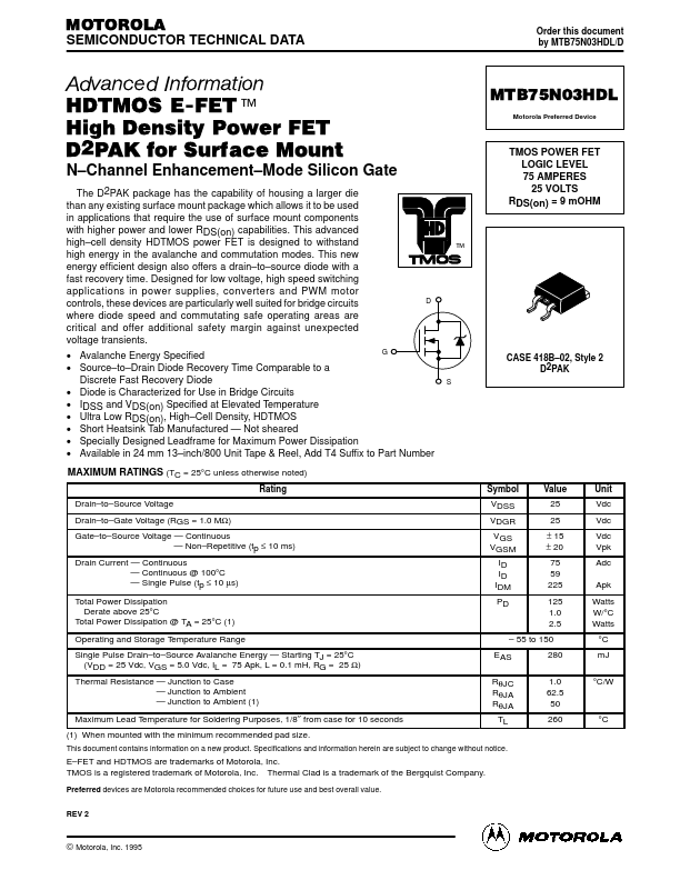
MOTOROLA
SEMICONDUCTOR TECHNICAL DATA
Order this document by MTB75N03HDL/D
Advanced Information
HDTMOS E-FET.™ High Density Power FET D2PAK for Surface Mount
N–Channel Enhancement–Mode Silicon Gate
The D2PAK package has the capability of housing a larger die than any existing surface mount package which allows it to be used in applications that require the use of surface mount components with higher power and lower RDS(on) capabilities. This advanced high–cell density HDTMOS power FET is designed to withstand high energy in the avalanche and commutation modes. This new energy efficient design also offers a drain–to–source diode with a fast recovery time.