Datasheet4U Logo Datasheet4U.com

MTB75N05HD - TMOS POWER FET

Key Features

  • unction of drain current, the mathematical solution is complex. The MOSFET output capacitance also complicates the mathematics. And finally, MOSFETs have finite internal gate resistance which effectively adds to the resistance of the driving source, but the internal resistance is difficult to measure and, consequently, is not specified. The resistive switching time variation versus gate resistance (Figure 9) shows how typical switching performance is affected by the parasitic circuit elements. I.

📥 Download Datasheet

Full PDF Text Transcription (Reference)

The following content is an automatically extracted verbatim text from the original manufacturer datasheet and is provided for reference purposes only.

View original datasheet text
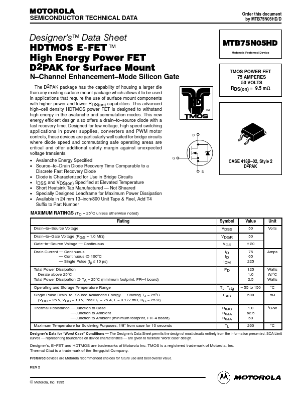
MOTOROLA SEMICONDUCTOR TECHNICAL DATA Order this document by MTB75N05HD/D ™ Data Sheet HDTMOS E-FET.™ High Energy Power FET D2PAK for Surface Mount Designer's MTB75N05HD Motorola Preferred Device N–Channel Enhancement–Mode Silicon Gate The D2PAK package has the capability of housing a larger die than any existing surface mount package which allows it to be used in applications that require the use of surface mount components with higher power and lower RDS(on) capabilities. This advanced high–cell density HDTMOS power FET is designed to withstand high energy in the avalanche and commutation modes. This new energy efficient design also offers a drain–to–source diode with a fast recovery time.