• Part: SN54LS112A
  • Description: DUAL JK NEGATIVE EDGE-TRIGGERED FLIP-FLOP
  • Manufacturer: Motorola Semiconductor
  • Size: 147.34 KB
Download SN54LS112A Datasheet PDF
Motorola Semiconductor
SN54LS112A
SN54LS112A is DUAL JK NEGATIVE EDGE-TRIGGERED FLIP-FLOP manufactured by Motorola Semiconductor.
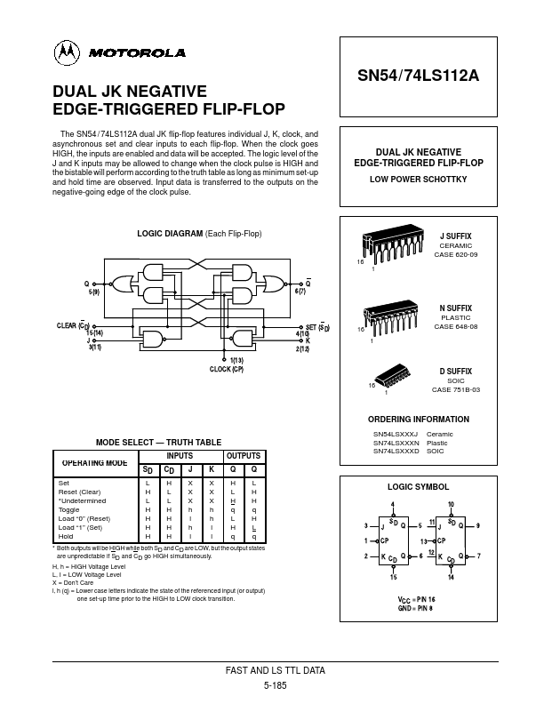
SN54/74LS112A DUAL JK NEGATIVE EDGE-TRIGGERED FLIP-FLOP The SN54 / 74LS112A dual JK flip-flop Features individual J, K, clock, and asynchronous set and clear inputs to each flip-flop. When the clock goes HIGH, the inputs are enabled and data will be accepted. The logic level of the J and K inputs may be allowed to change when the clock pulse is HIGH and the bistable will perform according to the truth table as long as minimum set-up and hold time are observed. Input data is transferred to the outputs on the negative-going edge of the clock pulse. DUAL JK NEGATIVE EDGE-TRIGGERED FLIP-FLOP LOW POWER SCHOTTKY LOGIC DIAGRAM (Each Flip-Flop) J SUFFIX CERAMIC CASE 620-09 16 1 Q 5(9) 6(7) CLEAR (CD) 15(14) J 3(11) 1(13) CLOCK (CP) 4(10) K 2(12) SET (SD) 16 1 N SUFFIX PLASTIC CASE 648-08 16 1 D SUFFIX SOIC CASE 751B-03 ORDERING INFORMATION MODE SELECT - TRUTH TABLE INPUTS OPERATING MODE SD Set Reset (Clear) - Undetermined Toggle Load “0” (Reset) Load “1” (Set) Hold L H L H H H H CD H L L H H H H J X X X h l h l K X X X h h l l Q H L H q L H q Q L H H q H L q OUTPUTS SN54LSXXXJ SN74LSXXXN SN74LSXXXD Ceramic Plastic SOIC LOGIC SYMBOL 4 10 J CP J CP 13 Q 6 12 - Both outputs will be HIGH while both SD and CD are LOW, but the output states are unpredictable if SD and CD go HIGH simultaneously. H, h = HIGH Voltage Level L, I = LOW Voltage Level X = Don’t Care l, h (q) = Lower case letters indicate the state of the referenced input (or output) l, h (q) = one set-up time prior to the HIGH to LOW clock transition. VCC = PIN 16 GND = PIN 8 FAST AND LS TTL DATA 5-185 SN54/74LS112A GUARANTEED OPERATING RANGES Symbol VCC TA IOH IOL Supply Voltage Operating Ambient Temperature Range Output...