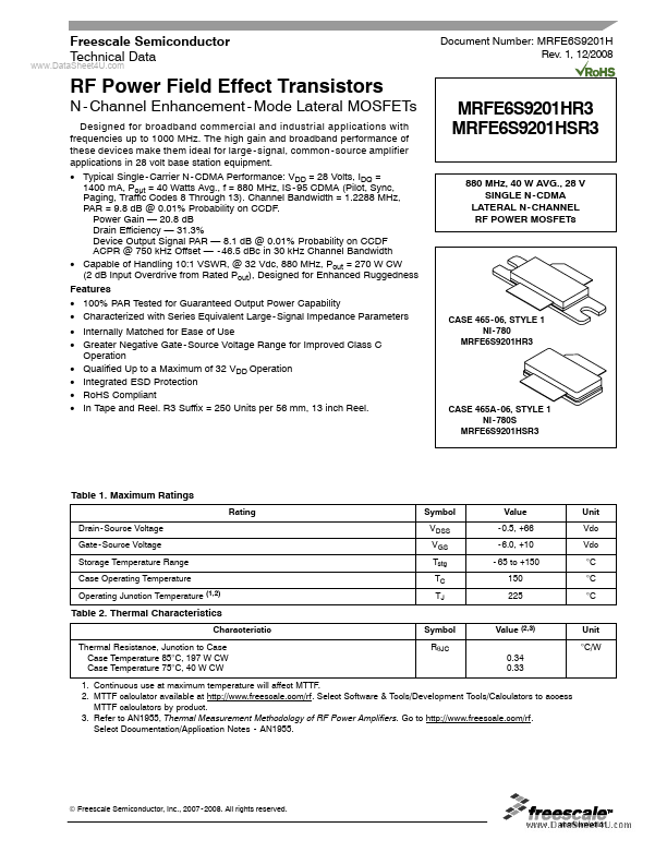
MRFE6S9201HR3
MRFE6S9201HR3 is RF Power Field Effect Transistors manufactured by Motorola Semiconductor.
..
Freescale Semiconductor Technical Data
Document Number: MRFE6S9201H Rev. 1, 12/2008
RF Power Field Effect Transistors
- Channel Enhancement
- Mode Lateral MOSFETs
Designed for broadband mercial and industrial applications with frequencies up to 1000 MHz. The high gain and broadband performance of these devices make them ideal for large
- signal, mon
- source amplifier applications in 28 volt base station equipment.
- Typical Single
- Carrier N
- CDMA Performance: VDD = 28 Volts, IDQ = 1400 m A, Pout = 40 Watts Avg., f = 880 MHz, IS
- 95 CDMA (Pilot, Sync, Paging, Traffic Codes 8 Through 13). Channel Bandwidth = 1.2288 MHz, PAR = 9.8 d B @ 0.01% Probability on CCDF. Power Gain
- 20.8 d B Drain Efficiency
- 31.3% Device Output Signal PAR
- 8.1 d B @ 0.01% Probability on CCDF ACPR @ 750 k Hz Offset
- - 46.5 d Bc in 30 k Hz Channel Bandwidth
- Capable of Handling 10:1 VSWR, @ 32 Vdc, 880 MHz, Pout = 270 W CW (2 d B Input Overdrive from Rated Pout), Designed for Enhanced Ruggedness Features
- 100% PAR Tested for Guaranteed Output Power Capability
- Characterized with Series Equivalent Large
- Signal Impedance Parameters
- Internally Matched for Ease of Use
- Greater Negative Gate
- Source Voltage Range for Improved Class C Operation
- Qualified Up to a Maximum of 32 VDD Operation
- Integrated ESD Protection
- Ro HS pliant
- In Tape and Reel. R3 Suffix = 250 Units per 56 mm, 13 inch Reel.
MRFE6S9201HR3 MRFE6S9201HSR3
880 MHz, 40 W AVG., 28 V SINGLE...