Datasheet4U Logo Datasheet4U.com

CS5825 - 28:4 LVDS Receiver

Description

CS5825 receives four LVDS data channels and one LVDS clock channel.

Each data channel is deserialized into 7-bit parallel data bus for output.

The clock channel is used for frame sync and fed into an internal PLL that generates the 7X serial clock used in the deserializer.

Features

  • CS5825 28:4 LVDS Receiver.
  • Four 7-bit serial data LVDS channels and one clock LVDS channel.
  • Compatible with ANSI TIA/EIA-644 LVDS standard.
  • Wide serial clocking speed ranges from 31MHz to 68MHz.
  • Support open-safe LVDS design.
  • Fully integrated on-chip PLL and digital phase alignment provide accurate deserializer operation.
  • Support power-down mode.
  • 5V/3.3V tolerant data input.
  • Single 3.3V supply operation.
  • C.

📥 Download Datasheet

Datasheet Details

Part number CS5825
Manufacturer Myson Technology
File Size 312.86 KB
Description 28:4 LVDS Receiver
Datasheet download datasheet CS5825 Datasheet

Full PDF Text Transcription (Reference)

The following content is an automatically extracted verbatim text from the original manufacturer datasheet and is provided for reference purposes only.

View original datasheet text
www.DataSheet4U.com Century Semiconductor Inc. 
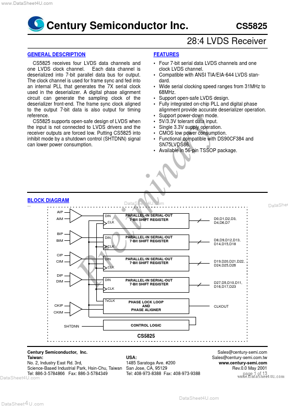
GENERAL DESCRIPTION CS5825 receives four LVDS data channels and one LVDS clock channel. Each data channel is deserialized into 7-bit parallel data bus for output. The clock channel is used for frame sync and fed into an internal PLL that generates the 7X serial clock used in the deserializer. A digital phase alignment circuit can generate the sampling clock of the deserializer front-end. The frame sync clock aligned to the output 7-bit data is also output for timing reference. CS5825 supports open-safe design of LVDS when the input is not connected to LVDS drivers and the receiver outputs are forced low. Putting CS5825 into inhibit mode by a shutdown control (SHTDNN) signal can lower power consumption.
Published: |