Download UPB429-1 Datasheet PDF
UPB429-1 page 2
Page 2
UPB429-1 page 3
Page 3

UPB429-1 Key Features

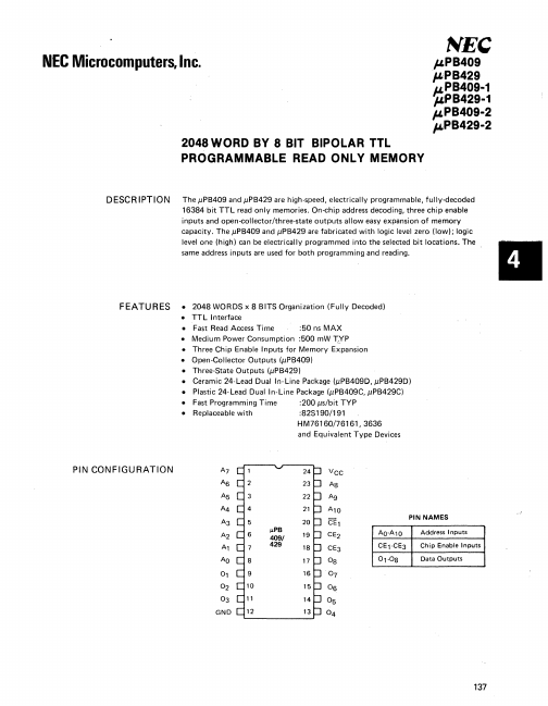
  • 2048 WORDS x 8 BITS Organization (Fully Decoded)
  • TT L Interface
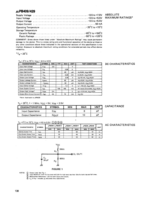
  • Fast Read Access Time
  • Medium Power Consumption :500 mW TyP
  • Three Chip Enable Inputs for Memory Expansion
  • Open-Collector Outputs (JlPB409)
  • Three-State Outputs (JlPB429)
  • Ceramic 24-Lead Dual In-Line Package (JlPB409D, JlPB429D)
  • Plastic

UPB429-1 Description

On-chip address decoding, three chip enable inputs and open-collector/three-state outputs allow easy expansion of memory capacity. The JlPB409 and JlPB429 are fabricated with logic level zero (low); logic level one (high) can be electrically programmed into the selected bit locations.