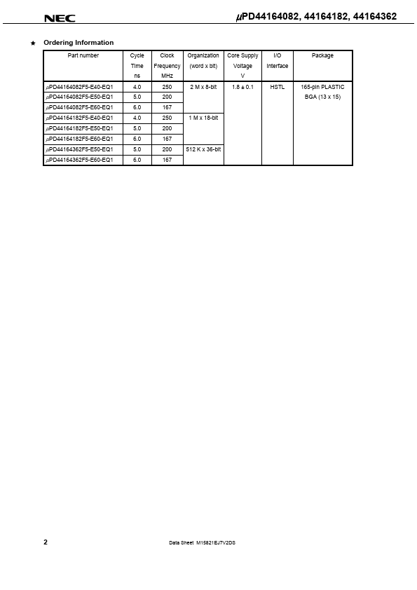
UPD44164082 Key Features
- 1.8 ± 0.1 V power supply and HSTL I/O
- DLL circuitry for wide output data valid window and future frequency scaling
- Pipelined double data rate operation
- mon data input/output bus
- Two-tick burst for low DDR transaction size
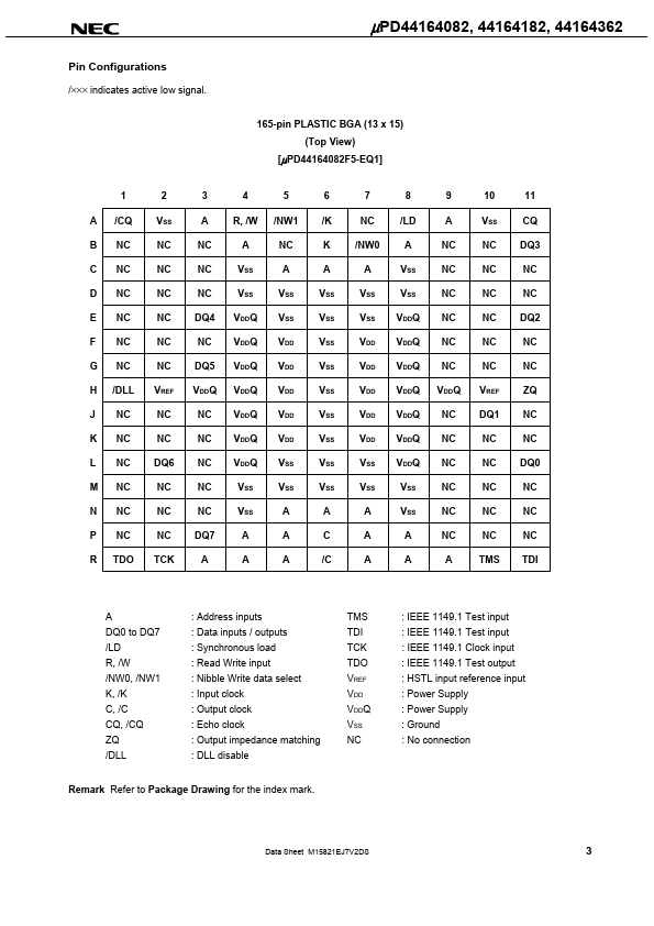
- Two input clocks (K and /K) for precise DDR timing at clock rising edges only
- Two output clocks (C and /C) for precise flight time and clock skew matching-clock and data delivered together to receiv
- Internally self-timed write control
- Clock-stop capability with µs restart
- User programmable impedance output