Datasheet Details
| Part number | LMH6503 |
|---|---|
| Manufacturer | National Semiconductor (now Texas Instruments) |
| File Size | 0.99 MB |
| Description | Wideband / Low Power / Linear Variable Gain Amplifier |
| Datasheet |
 LMH6503 Datasheet LMH6503 Datasheet
|
|
|
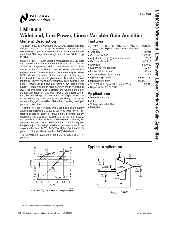
The LMH™6503 is a wideband DC coupled differential input voltage controlled gain stage followed by a high-speed current feedback Op Amp which can directly drive a low impedance load.
Gain adjustment range is more than 70dB for up to 10MHz.
| Part number | LMH6503 |
|---|---|
| Manufacturer | National Semiconductor (now Texas Instruments) |
| File Size | 0.99 MB |
| Description | Wideband / Low Power / Linear Variable Gain Amplifier |
| Datasheet |
LMH6503 Datasheet
|
|
|
|