EB201
EB201 is High Cell Density MOSFET manufactured by onsemi.
..
EB201/D High Cell Density MOSFETs
Low On- Resistance Affords New Design Options
Prepared by: Kim Gauen and Wayne Chavez ON Semiconductor http://onsemi.
ENGINEERING BULLETIN
Just a few years ago an affordable 60 V, 10 mΩ power transistor was a dream. After all, 10 mΩ is the resistance of about 20 cm of #22 gauge wire. Today a sub- 10 mΩ power MOSFET is not only available, it is housed in a standard TO- 220. Such are the advances that have occurred lately in “high cell density” power MOSFET technology. Furthermore, Motorola’s high cell density technology, HDTMOS®, brings other advantages such as greatly improved body diode performance. The technological advances are sufficiently great that they are fundamentally changing low voltage power transistor technology.
Cutting the MOSFET’s On- Resistance
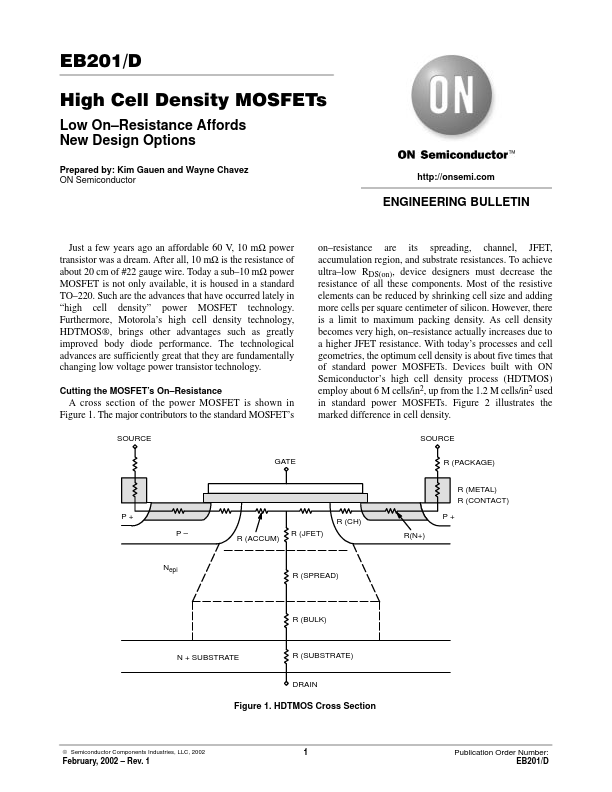
A cross section of the power MOSFET is shown in Figure 1. The major contributors to the standard MOSFET’s
SOURCE GATE on- resistance are its spreading, channel, JFET, accumulation region, and substrate resistances. To achieve ultra- low RDS(on), device designers must decrease the resistance of all these ponents. Most of the resistive elements can be reduced by shrinking cell size and adding more cells per square centimeter of silicon. However, there is a limit to maximum packing density. As cell density bees very high, on- resistance actually increases due to a higher JFET resistance. With today’s processes and cell geometries, the optimum cell density is about five times that of standard power MOSFETs. Devices built with ON Semiconductor’s high cell density process (HDTMOS) employ about 6 M cells/in2, up from the 1.2 M cells/in2 used in standard power MOSFETs. Figure 2 illustrates the marked difference in cell density.
SOURCE R (PACKAGE) R (METAL) R (CONTACT)
P+ P- R (ACCUM) R (JFET)
R (CH) R(N+)
P+
Nepi
R (SPREAD)
R (BULK)
N + SUBSTRATE
R (SUBSTRATE)
DRAIN
Figure 1. HDTMOS Cross Section
© Semiconductor ponents Industries, LLC,...