FDC642P
FDC642P is P-Channel MOSFET manufactured by onsemi.
Features
General Description
- Max r DS(on) = 65 mΩ at VGS = -4.5 V, ID = -4.0 A
- Max r DS(on) = 100 mΩ at VGS = -2.5 V, ID = -3.2 A
- Fast switching speed
- Low gate charge (11n C typical)
- High performance trench technology for extremely low r DS(on)
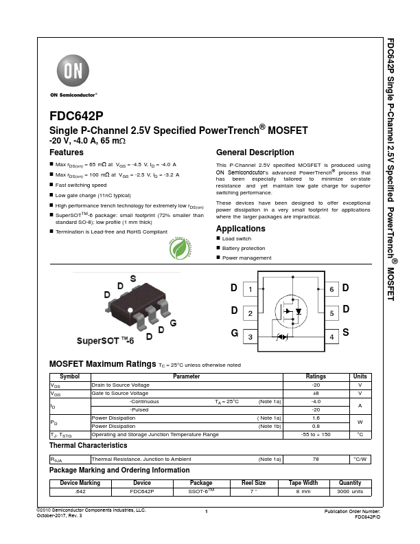
- Super SOTTM-6 package: small footprint (72% smaller than standard SO-8); low profile (1 mm thick)
- Termination is Lead-free and Ro HS pliant
This P-Channel 2.5V specified MOSFET is produced using ON Semicondcutor’s advanced Power Trench® process that has been especially tailored to minimize on-state resistance and yet maintain low gate charge for superior switching performance.
These devices have been designed to offer exceptional power dissipation in a very small footprint for applications where the larger packages are impractical.
Applications
- Load switch
- Battery protection
- Power management
MOSFET Maximum Ratings TC = 25°C unless otherwise noted
Symbol VDS VGS ID
PD TJ, TSTG
Parameter
Drain to Source Voltage
Gate to Source Voltage
-Continuous -Pulsed
TA = 25°C
Power Dissipation
Power Dissipation
Operating and Storage Junction Temperature Range
Thermal Characteristics
(Note 1a)
( Note 1a) (Note 1b)
Ratings -20 ±8 -4.0 -20 1.6 0.8
-55 to + 150
Units V V A
W...