FDZ1905PZ
Overview
This device is designed specifically as a single package solution for the battery charge switch in cellular handset and other ultra-portable applications. It features two common drain P-channel MOSFETs, which enables bidirectional current flow, on ON Semiconductor’s advanced 1.5 V POWERTRENCH process with state of the art “low pitch” WLCSP packaging process, the FDZ1905PZ minimizes both PCB space and rS1S2(on).
- Max rS1S2(on) = 126 mW at VGS = -4.5 V, IS1S2 = -1 A
- Max rS1S2(on) = 141 mW at VGS = -2.5 V, IS1S2 = -1 A
- Max rS1S2(on) = 198 mW at VGS = -1.8 V, IS1S2 = -1 A
- Max rS1S2(on) = 303 mW at VGS = -1.5 V, IS1S2 = -1 A
- Occupies only 1.5 mm2 of PCB area, less than 50% of the area of 2 x 2 BGA
- Ultra-thin package: less than 0.65 mm height when mounted to PCB
- High power and current handling capability
- HBM ESD protection level > 4 kV (Note 3)
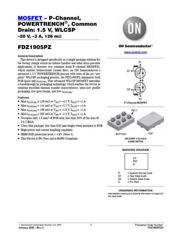
- This Device is Pb-Free and is RoHS Compliant S1 G1 G2 S2 P-Channel MOSFET PIN 1 S1 S1 G1 G2 S2 S2 BOTTOM TOP WLCSP6 1.5x1x0.6 CASE 567PW