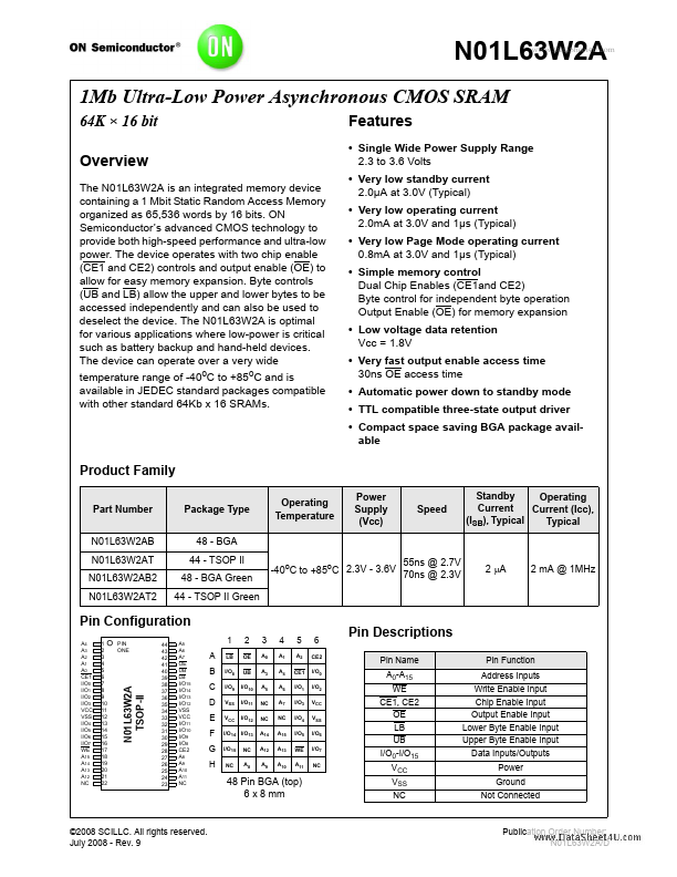
Datasheet4U Logo Datasheet4U.com

N01L63W2A - Ultra-Low Power Asynchronous CMOS SRAM

Description

Pin Name A0-A15 WE CE1, CE2 OE LB UB I/O0-I/O15 VCC VSS NC Pin Function Address Inputs Write Enable Input Chip Enable Input Output Enable Input Lower Byte Enable Input Upper Byte Enable Input Data Inputs/Outputs Power Ground Not Connected N01L63W2A TSOP-II I/O14 I/O13 I/O15 NC NC A8 48 Pin BGA (

Features

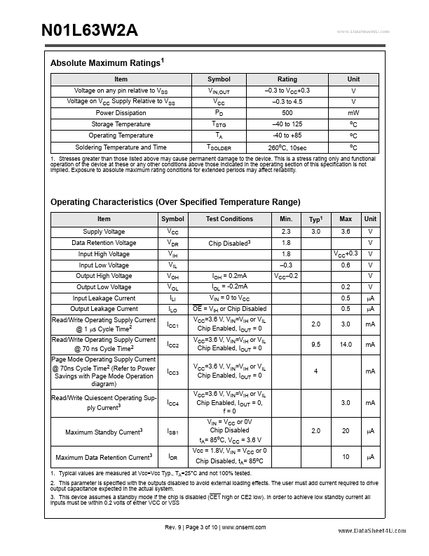
  • Single Wide Power Supply Range 2.3 to 3.6 Volts.
  • Very low standby current 2.0µA at 3.0V (Typical).
  • Very low operating current 2.0mA at 3.0V and 1µs (Typical).
  • Very low Page Mode operating current 0.8mA at 3.0V and 1µs (Typical).
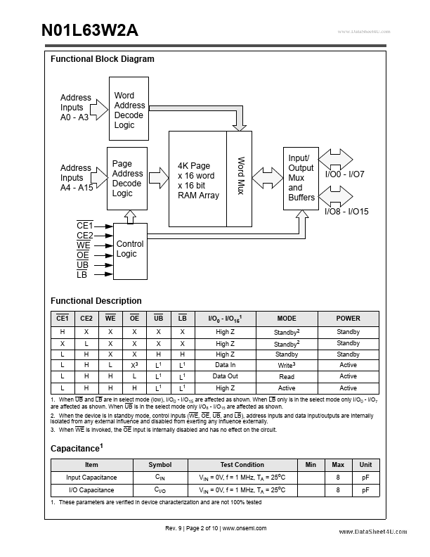
  • Simple memory control Dual Chip Enables (CE1and CE2) Byte control for independent byte operation Output Enable (OE) for memory expansion.
  • Low voltage data retention Vcc = 1.8V.
  • Very fast output enable access.

📥 Download Datasheet

Datasheet Details

Part number N01L63W2A
Manufacturer onsemi
File Size 240.54 KB
Description Ultra-Low Power Asynchronous CMOS SRAM
Datasheet download datasheet N01L63W2A Datasheet

Full PDF Text Transcription

Click to expand full text
N01L63W2A 1Mb Ultra-Low Power Asynchronous CMOS SRAM 64K × 16 bit Overview The N01L63W2A is an integrated memory device containing a 1 Mbit Static Random Access Memory organized as 65,536 words by 16 bits. ON Semiconductor’s advanced CMOS technology to provide both high-speed performance and ultra-low power. The device operates with two chip enable (CE1 and CE2) controls and output enable (OE) to allow for easy memory expansion. Byte controls (UB and LB) allow the upper and lower bytes to be accessed independently and can also be used to deselect the device. The N01L63W2A is optimal for various applications where low-power is critical such as battery backup and hand-held devices.
Published: |