Datasheet4U Logo Datasheet4U.com

NB4N855S Datasheet Dual AnyLevel to LVDS Receiver/Driver/Buffer/Translator

Manufacturer: onsemi

Datasheet Details

Part number NB4N855S
Manufacturer onsemi
File Size 203.55 KB
Description Dual AnyLevel to LVDS Receiver/Driver/Buffer/Translator
Datasheet download datasheet NB4N855S Datasheet

General Description

NB4N855S is a clock or data Receiver/Driver/Buffer/Translator capable of translating AnyLevel input signal (LVPECL, CML, HSTL, LVDS, or LVTTL/LVCMOS) to LVDS.

Depending on the distance, noise immunity of the system design, and transmission line media, this device will receive, drive or translate data or clock signals up to 1.5 Gb/s or 1.0 GHz, respectively.

This device is pin−for−pin plug in compatible to the SY55855V in a 3.3 V applications.

Overview

NB4N855S 3.3 V, 1.5 Gb/s Dual AnyLevel™ to LVDS Receiver/Driver/Buffer/.

Key Features

  • Guaranteed Input Clock Frequency up to 1.0 GHz.
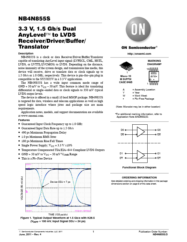
  • Guaranteed Input Data Rate up to 1.5 Gb/s.
  • 490 ps Maximum Propagation Delay.
  • 1.0 ps Maximum RMS Jitter.
  • 180 ps Maximum Rise/Fall Times.
  • Single Power Supply; VCC = 3.3 V ±10%.
  • Temperature Compensated TIA/EIA.
  • 644 Compliant LVDS Outputs.
  • GND + 50 mV to VCC.
  • 50 mV VCMR Range.
  • This is a Pb.
  • Free Device http://onsemi. com 1 Micro.
  • 10 M SUFFIX.