Datasheet4U Logo Datasheet4U.com

NB4N111K - Clock Fanout Buffer

Datasheet Summary

Description

buffer, optimized for ultra low propagation delay variation.

The NB4N111K is designed with HCSL clock distribution for FBDIMM applications in mind.

ended LVPECL,

Features

  • Typical Input Clock Frequencies: 100, 133, 166, 200, 266, 333, and 400 MHz.
  • 340 ps Typical Rise and Fall Times.
  • 800 ps Typical Propagation Delay.
  • Dtpd 100 ps Maximum Propagation Delay Variation Per Each Differential Pair.

📥 Download Datasheet

Datasheet preview – NB4N111K

Datasheet Details

Part number NB4N111K
Manufacturer ON Semiconductor
File Size 223.23 KB
Description Clock Fanout Buffer
Datasheet download datasheet NB4N111K Datasheet
Additional preview pages of the NB4N111K datasheet.
Other Datasheets by ON Semiconductor

Full PDF Text Transcription

Click to expand full text
NB4N111K Clock Fanout Buffer, 1:10 Differential, 3.3 V, with HCSL Level Output Description The NB4N111K is a differential input clock 1 to 10 HCSL fanout buffer, optimized for ultra low propagation delay variation. The NB4N111K is designed with HCSL clock distribution for FBDIMM applications in mind. Inputs can accept differential VLPECL, CML, or VLDS levels.Single −
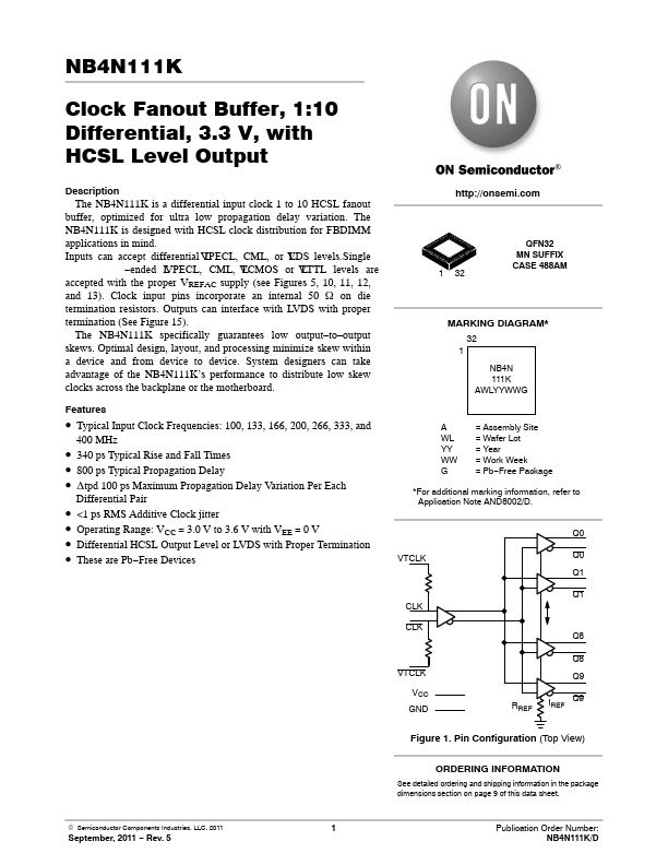
ended LVPECL, CML, VLCMOS or VLTTL levels are accepted with the proper VREFAC supply (see Figures 5, 10, 11, 12, and 13). Clock input pins incorporate an internal 50 W on die termination resistors. Outputs can interface with LVDS with proper termination (See Figure 15). The NB4N111K specifically guarantees low output–to–output skews.
Published: |