Datasheet4U Logo Datasheet4U.com

NB4N121K - 3.3V Differential 1:21 Differential Fanout Clock Driver

Datasheet Summary

Description

21 HCSL level differential outputs, optimized for ultra low propagation delay variation.

The NB4N121K is designed with HCSL clock distribution for FBDIMM applications in mind.

Features

  • Typical Input Clock Frequency 100, 133, 166, 200, 266, 333 and 400 MHz.
  • 340 ps Typical Rise and Fall Times.
  • 800 ps Typical Propagation Delay.
  • Dtpd 100 ps Maximum Propagation Delay Variation Per Each Differential Pair.
  • Additive Phase RMS Jitter: 1 ps Max.
  • Operating Range: VCC = 3.0 V to 3.6 V with VEE = 0 V.
  • Differential HCSL Output Level (700 mV Peak.
  • to.
  • Peak).
  • These Devices are Pb.
  • Free, Halogen Free/.

📥 Download Datasheet

Datasheet preview – NB4N121K

Datasheet Details

Part number NB4N121K
Manufacturer ON Semiconductor
File Size 204.36 KB
Description 3.3V Differential 1:21 Differential Fanout Clock Driver
Datasheet download datasheet NB4N121K Datasheet
Additional preview pages of the NB4N121K datasheet.
Other Datasheets by ON Semiconductor

Full PDF Text Transcription

Click to expand full text
3.3 V Differential 1:21 Differential Fanout Clock Driver with HCSL level Output NB4N121K Description The NB4N121K is a Clock differential input fanout distribution 1 to 21 HCSL level differential outputs, optimized for ultra low propagation delay variation. The NB4N121K is designed with HCSL clock distribution for FBDIMM applications in mind. Inputs can accept differential LVPECL, CML, or LVDS levels. Single−ended LVPECL, CML, LVCMOS or LVTTL levels are accepted with the proper VREFAC supply (see Figures 5, 10, 11, 12, and 13). Clock input pins incorporate an internal 50 W on die termination resistors. 
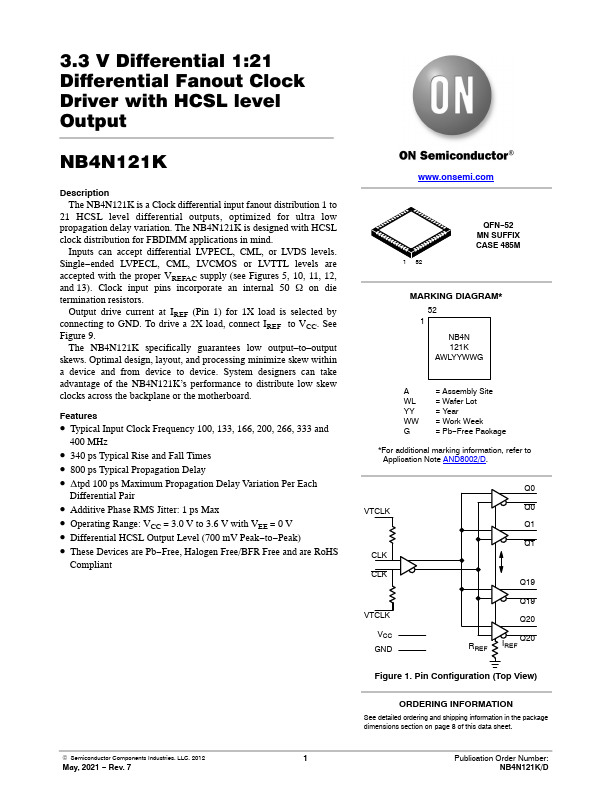
Output drive current at IREF (Pin 1) for 1X load is selected by connecting to GND. To drive a 2X load, connect IREF to VCC. See Figure 9.
Published: |