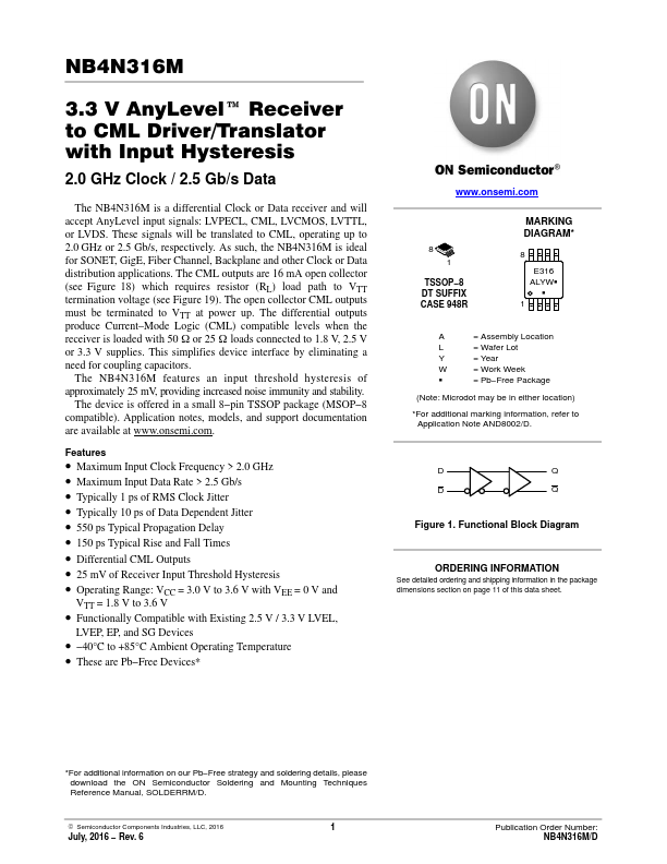
Datasheet4U Logo Datasheet4U.com
onsemi logo

NB4N316M Datasheet

Manufacturer: onsemi
NB4N316M datasheet preview

Datasheet Details

Part number NB4N316M
Datasheet NB4N316M_ONSemiconductor.pdf
File Size 225.76 KB
Manufacturer onsemi
Description AnyLevel Receiver to CML Driver/Translator
NB4N316M page 2 NB4N316M page 3

NB4N316M Overview

Pin Name I/O Description 1 NC − No Connect. 2 D ECL, CML, LVCMOS, LVDS, Noninverted Differential Input. (Note 1) LVTTL Input 3 D ECL, CML, LVCMOS, LVDS, Inverted Differential Input.

NB4N316M Key Features

  • Maximum Input Clock Frequency > 2.0 GHz
  • Maximum Input Data Rate > 2.5 Gb/s
  • Typically 1 ps of RMS Clock Jitter
  • Typically 10 ps of Data Dependent Jitter
  • 550 ps Typical Propagation Delay
  • 150 ps Typical Rise and Fall Times
  • Differential CML Outputs
  • 25 mV of Receiver Input Threshold Hysteresis
  • Operating Range: VCC = 3.0 V to 3.6 V with VEE = 0 V and
  • Functionally patible with Existing 2.5 V / 3.3 V LVEL
onsemi logo - Manufacturer

More Datasheets from onsemi

See all onsemi datasheets

Part Number Description
NB4N111K Clock Fanout Buffer
NB4N1158 Link Replicator
NB4N11M Multi Level Clock/Data Input to CML Receiver/Buffer/Translator
NB4N11S 3.3V 1:2 AnyLevel Input to LVDS Fanout Buffer /Translator
NB4N121K 3.3V Differential 1:21 Differential Fanout Clock Driver
NB4N441 3.3V Serial Input MultiProtocol PLL Clock Synthesizer
NB4N507A PECL Clock Synthesizer
NB4N527S Dual AnyLevel to LVDS Receiver/Driver/Buffer/Translator
NB4N7132 Link Replicator
NB4N840M 3.3V 3.2Gb/s Dual Differential Clock/Data 2 x 2 Crosspoint Switch

NB4N316M Distributor

Datasheet4U Logo
Since 2006. D4U Semicon. About Datasheet4U Contact Us Privacy Policy Purchase of parts