NCD57255
NCD57255 is Isolated Dual Channel IGBT/MOSFET Gate Driver manufactured by onsemi.
- Part of the NCD57252 comparator family.
- Part of the NCD57252 comparator family.
Features
- High Peak Output Current (±6.5 A- , ±3.5 A- )
- Configurable as a Dual Low- Side or Dual High- Side or Half- Bridge
Driver
- Programmable Overlap or Dead Time control
- Disable Pin to Turn Off Outputs for Power Sequencing
- ANB Function to Offer Flexibility to Set up the Driver as
Half- bridge Driver Operating with a Single Input Signal
- IGBT/MOSFET Gate Clamping during Short Circuit
- Short Propagation Delays with Accurate Matching
- Tight UVLO Thresholds on all Power Supplies
- 3.3 V, 5 V, and 15 V Logic Input
- 2.5 or 5 k Vrms- Galvanic Isolation from Input to each Output and 1.5 k Vrms Differential Voltage between Output Channels
- 1200 V Working Voltage (per VDE0884- 11 Requirements)
- High mon Mode Transient Immunity
- NCV Prefix for Automotive and Other Applications Requiring
Unique Site and Control Change Requirements; AEC- Q100 Qualified and PPAP Capable
- This Device is Pb- Free, Halogen Free/BFR Free and is Ro HS pliant
Typical Applications
- EV Chargers
- Motor Control
- Uninterruptible Power Supplies (UPS)
- Industrial Power Supplies
- Solar Inverters
- Automotive Applications
- Depends on package variant, see Page 6, 21.
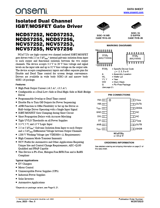
SOIC- 16 WB CASE 751G- 03
SOIC- 16 D SUFFIX CASE 751B- 05
MARKING DIAGRAMS 16
5725y AWLYYWWG
5725y AWLYWWG
5725y = Specific Device Code y = 2, 3, 5 or 6
= Assembly Location
= Wafer Lot
YY, Y =...