PI6C2404A-1
Description
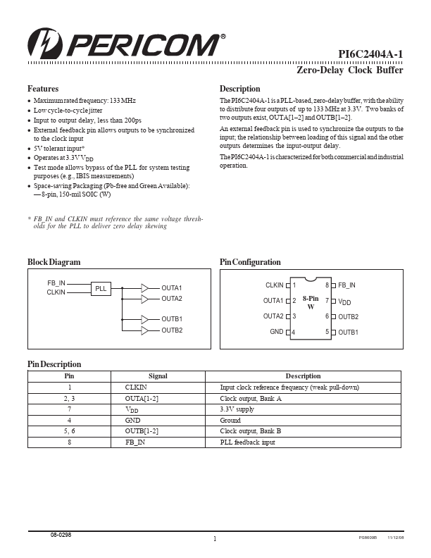
The PI6C2404A-1 is a PLL-based, zero-delay buffer, with the ability to distribute four outputs of up to 133 MHz at 3.3V.
Key Features
- Maximum rated frequency: 133 MHz
- Low cycle-to-cycle jitter
- Input to output delay, less than 200ps
- External feedback pin allows outputs to be synchronized to the clock input
- 5V tolerant input*
- Operates at 3.3V VDD
- Test mode allows bypass of the PLL for system testing purposes (e.g., IBIS measurements)
- Space-saving Packaging (Pb-free and Green Available): - 8-pin, 150-mil SOIC (W)