PI6C2504
PI6C2504 is Phase-Locked Loop Clock Driver manufactured by Pericom Semiconductor.
Features
- High-Performance Phase-Locked-Loop Clock Distribution for Networking
- Registered DIMM Synchronous DRAM modules for server/workstation/PC applications
- Allows Clock Input to have Spread Spectrum modulation for EMI reduction
- Zero Input-to-Output delay
- Low jitter: Cycle-to-Cycle jitter ±100ps max.
- On-chip series damping resistor at clock output drivers for low noise and EMI reduction
- Operates at 3.3V VCC
- Wide range of Clock Frequencies up to 80 MHz
- Package: Plastic 16-pin QSOP Package (Q)
Product Description
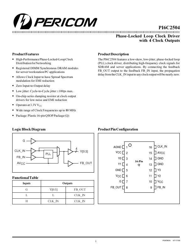
The PI6C2504 features a low-skew, low-jitter, phase-locked loop (PLL) clock driver, distributing high-frequency clock signals for SDRAM and server applications. By connecting the feedback FB_OUT output to the feedback FB_IN input, the propagation delay from the CLK_IN input to any clock output will be nearly zero.
Logic Block Diagram
G 4 PLL FB_IN AVCC FB_OUT Y[0:3]
Product Pin Configuration
AGND VCC Y0 Y1 GND
1 2 3 4 5 6 7 8
16 15
CLK_IN AVCC GND GND Y3 Y2 VCC FB_IN
CLK_IN
16-Pin Q
14 13 12 11 10 9
Functional Table
Inputs G L H Y[0:3] L CLK _IN Outputs FB_O UT CLK _IN CLK _IN
VCC G FB_OUT
PS8380A
07/17/00
PI6C2504 Phase-Locked Loop Clock Driver with 4 Clock Outputs 12345678901234567890123456789012123456789012345678901234567890121234567890123456789012345678901212345678901234567890123456789012123456789012 Pin Functions
Pin Name CLK _IN FB_IN G FB_O UT Y[0:3] AVC C AGND VC C GND Pin No. 16 9 7 8 3,4,11,12 15 1 2, 6, 10 5, 13, 14 Type I I I O O Power Ground Power Ground D e s cription Reference Clock input. CLK _IN allows spread spectrum clock input. Feedback input. FB_IN provides the feedback signal to the internal PLL. O utput bank enable. When G is LO W, outputs Y[0:3] are disabled to a logic low state. Feedback output. FB_O UT is dedicated for external feedback. FB_O UT has an embedded series- damping resistor of the same value as the clock outputs Yx. C lock outputs. These outputs provide low- skew copies of CLK _IN...