Datasheet4U Logo Datasheet4U.com

PI6C2404A-1 - Zero-Delay Clock Buffer

General Description

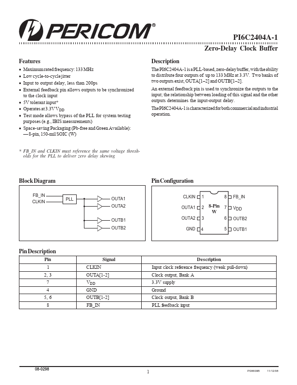
The PI6C2404A-1 is a PLL-based, zero-delay buffer, with the ability to distribute four outputs of up to 133 MHz at 3.3V.

2] and OUTB[1

2].

Key Features

  • Maximum rated frequency: 133 MHz.
  • Low cycle-to-cycle jitter.
  • Input to output delay, less than 200ps.
  • External feedback pin allows outputs to be synchronized to the clock input.
  • 5V tolerant input.
  • Operates at 3.3V VDD.
  • Test mode allows bypass of the PLL for system testing purposes (e. g. , IBIS measurements).
  • Space-saving Packaging (Pb-free and Green Available):.
  • 8-pin, 150-mil SOIC (W).

📥 Download Datasheet

Full PDF Text Transcription (Reference)

The following content is an automatically extracted verbatim text from the original manufacturer datasheet and is provided for reference purposes only.

View original datasheet text
PI6C2404A-11122334455667788990011223344556677889900112233445566778899001122112233445566778899001122334455667788990011223344556677889900112211223344556677889900112233445566778899001122334455667788990011221122334455667788990011223344556677889900112233445566778899001122112233445566778899001122 Zero-Delay Clock Buffer Features • Maximum rated frequency: 133 MHz • Low cycle-to-cycle jitter • Input to output delay, less than 200ps • External feedback pin allows outputs to be synchronized to the clock input • 5V tolerant input* • Operates at 3.3V VDD • Test mode allows bypass of the PLL for system testing purposes (e.g.