PI6C2501
PI6C2501 is Phase-Locked Loop Clock Driver manufactured by Pericom Semiconductor.
Features
- High-Performance, Phase-Locked-Loop Clock Distribution
- Allows Clock Input to have Spread Spectrum modulation for EMI reduction
- Zero Input-to-Output delay
- Low jitter: Cycle-to-Cycle jitter ±100ps max.
- On-chip series damping resistor at clock output drivers for low noise and EMI reduction
- Operates at 3.3V VCC
- Wide range of Clock Frequencies up to 80 MHz
- Package: Plastic 8-pin SOIC (W)
Product Description
The PI6C2501 features a low-skew, low-jitter, phase-locked loop (PLL) clock driver. By connecting the CLK_OUT output to the feedback FB_IN input, the propagation delay from the CLK_IN input to CLK_OUT output will be nearly zero.
Application
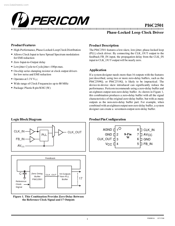
If a system designer needs more than 16 outputs with the features just described, using two or more zero-delay buffers, such as the PI6C2509Q, or PI6C2510Q, is likely to be impractical. The device-to-device skew introduced can significantly reduce the performance. Peri remends using a zero-delay buffer and an eighteen output non-zero-delay buffer. As shown in Figure 1, this bination produces a zero-delay buffer with all the signal characteristics of the original zero-delay buffer, but with as many outputs as the non-zero-delay buffer part. For example, when bined with an eighteen output non-zero delay buffer, a system designer can create a seventeen-output zero-delay buffer.
Logic Block Diagram
Product Pin Configuration
AGND GND CLK_OUT VCC 1 2 3 4 8 7 6 5 CLK_IN AVCC GND FB_IN
CLK_IN PLL FB_IN AVCC
CLK_OUT
8-Pin W
Feedback
Reference Clock Signal
Zero Delay Buffer PI6C2501
CLK_OUT
18 Outputs Non-PLL Buffer
Figure 1. This bination Provides Zero-Delay Between the Reference Clock Signal and 17 Outputs
PS8381A
07/17/00
PI6C2501 Phase-Locked Loop Clock Driver 12345678901234567890123456789012123456789012345678901234567890121234567890123456789012345678901212345678901234567890123456789012123456789012 Pin Functions
Pin Name CLK _IN FB_IN CLK _O UT AVC C AGND VC C GND Pin No. 8 5 3 7 1 4...