Datasheet4U Logo Datasheet4U.com

PI90LVB044 - LVDS Dual 2x2 Crosspoint/Repeater Switch

Download the PI90LVB044 datasheet PDF (PI90LV044 included). The manufacturer datasheet provides complete specifications, pinout details, electrical characteristics, and typical applications for lvds dual 2x2 crosspoint/repeater switch.

Description

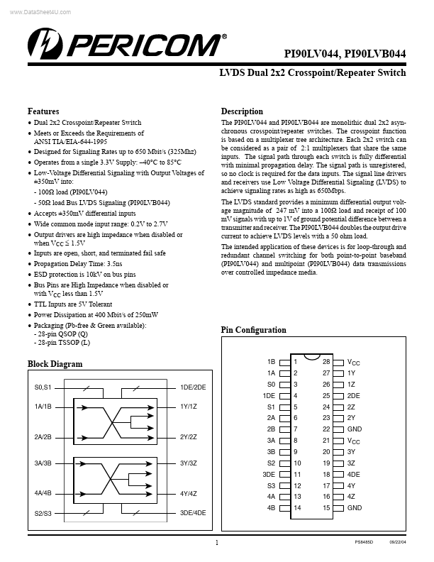
The PI90LV044 and PI90LVB044 are monolithic dual 2x2 asynchronous crosspoint/repeater switches.

The crosspoint function is based on a multiplexer tree architecture.

Each 2x2 switch can be considered as a pair of 2:1 multiplexers that share the same inputs.

Features

  • Dual 2x2 Crosspoint/Repeater Switch.
  • Meets or Exceeds the Requirements of ANSI TIA/EIA-644-1995.
  • Designed for Signaling Rates up to 650 Mbit/s (325Mhz).
  • Operates from a single 3.3V Supply:.
  • 40°C to 85°C.
  • Low-Voltage Differential Signaling with Output Voltages of ±350mV into: - 100Ω load (PI90LV044) - 50Ω load Bus LVDS Signaling (PI90LVB044).
  • Accepts ±350mV differential inputs.
  • Wide common mode input range: 0.2V to 2.7V.

📥 Download Datasheet

Note: The manufacturer provides a single datasheet file (PI90LV044_PericomSemiconductor.pdf) that lists specifications for multiple related part numbers.

Datasheet Details

Part number PI90LVB044
Manufacturer Pericom Semiconductor
File Size 463.08 KB
Description LVDS Dual 2x2 Crosspoint/Repeater Switch
Datasheet download datasheet PI90LVB044 Datasheet
Other Datasheets by Pericom Semiconductor

Full PDF Text Transcription

Click to expand full text
www.DataSheet4U.com PI90LV044, PI90LVB044 LVDS Dual 2x2 Crosspoint/Repeater Switch Features • Dual 2x2 Crosspoint/Repeater Switch • Meets or Exceeds the Requirements of ANSI TIA/EIA-644-1995 • Designed for Signaling Rates up to 650 Mbit/s (325Mhz) • Operates from a single 3.3V Supply: –40°C to 85°C • Low-Voltage Differential Signaling with Output Voltages of ±350mV into: - 100Ω load (PI90LV044) - 50Ω load Bus LVDS Signaling (PI90LVB044) • Accepts ±350mV differential inputs • Wide common mode input range: 0.2V to 2.7V • Output drivers are high impedance when disabled or when VCC ≤ 1.5V • Inputs are open, short, and terminated fail safe • Propagation Delay Time: 3.5ns • ESD protection is 10kV on bus pins • Bus Pins are High Impedance when disabled or with VCC less than 1.
Published: |