Datasheet4U.com
🌙
PNMT3400 Datasheet | Prisemi
Part:
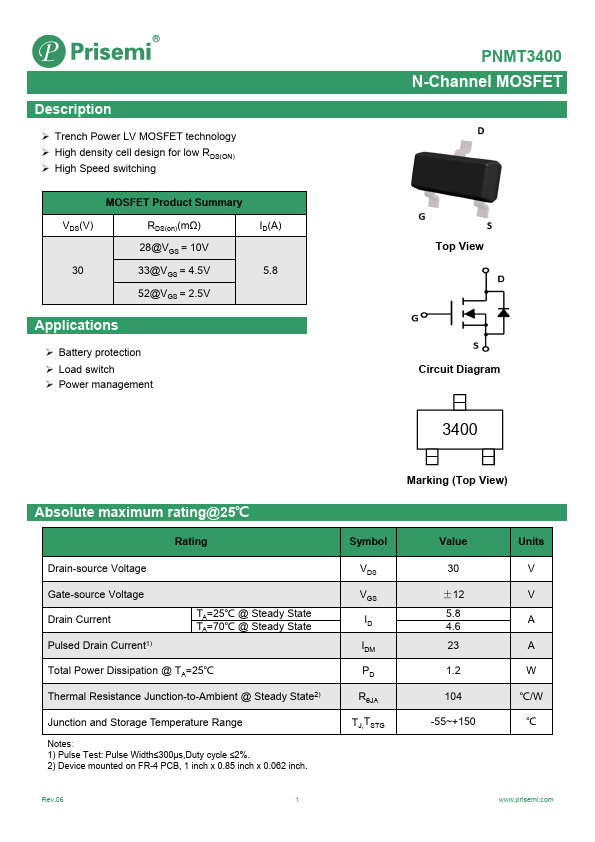
PNMT3400
Description:
N-Channel MOSFET
Category:
MOSFET
Manufacturer:
Prisemi
Size:
1.15 MB
PNMT3400 Datasheet (PDF) Download
Prisemi
PNMT3400
Description
.
Applications
Battery protection
×
Close