8P34S2102
8P34S2102 is Dual 1:2 LVDS Output 1.8V Fanout Buffer manufactured by Renesas.
Description
The 8P34S2102 is a high-performance, low-power, differential dual 1:2 LVDS output, 1.8V fanout buffer. The device is designed for the fanout of high-frequency, very low additive phase-noise clock and data signals.
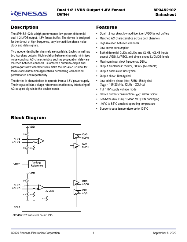
Two independent buffer channels are available. Each channel has two low-skew outputs. High isolation between channels minimizes noise coupling. AC characteristics such as propagation delay are matched between channels. Guaranteed output-to-output and part-to-part skew characteristics make the 8P34S2102 ideal for those clock distribution applications demanding well-defined performance and repeatability.
The device is characterized to operate from a 1.8V power supply. The integrated bias voltage references enable easy interfacing of AC-coupled signals to the device inputs.
Features
- Dual 1:2 low skew, low additive jitter LVDS fanout buffers
- Matched AC characteristics across both channels
- High isolation between channels
- Low power consumption
- Both differential CLKA, n CLKA and CLKB, n CLKB inputs accept LVDS, LVPECL and single-ended LVCMOS levels
- Maximum input clock frequency: 2GHz
- Output amplitudes: 350m V, 500m V (selectable)
- Output bank skew: 8ps typical
- Output skew: 10ps typical
- Low additive phase jitter, RMS: 45fs typical
(f REF = 156.25MHz, 12k Hz
- 20MHz)
- Full 1.8V supply voltage mode
- Device current consumption (IDD): 76m A typical
- Lead-free (Ro HS 6), 16-lead VFQFPN packaging
- -40°C to 85°C ambient operating temperature
- Supports case temperature up to 105°C
Block Diagram
51k
CLKA n CLKA
51k 51k
QA0 n QA0
QA1 n QA1
VREF
Voltage Reference
51k
CLKB n CLKB
51k 51k
51k
SELA
8P34S2102 transistor count: 293
QB0 n...