8V19N880
8V19N880 is RF Sampling Clock Generator and Jitter Attenuator manufactured by Renesas.
Features
- High-performance clock RF sampling clock generator and clock jitter attenuator with support for JESD204B/C
- Low phase noise: -144.7d Bc/Hz (800k Hz offset; 491.52MHz)
- Integrated phase noise of 74fs RMS (12k-20MHz, 491.52MHz)
- Dual-PLL architecture with internal and optional external VCO
- Eight output channels with a total of 18 outputs
- Configurable integer clock frequency dividers
- Clock output frequencies: up to 3932.16MHz
(Internal VCO) and 6GHz (optional external VCO)
- Differential, low noise I/O
- Deterministic phase delay and integrated phase delay circuits
- Redundant input clock architecture with four inputs and monitors, holdover, and input switching
- SPI 3/4 wire configuration interface
- Supply voltage: 1.8V and 3.3V
- Package: 100 CABGA (11 x 11 mm²)
- Temperature range: -40°C to +95°C (board)
Applicable Standards
- JESD204B and C
Applications
- Wireless infrastructure applications: 4G, 5G, and mm Wave
- Data acquisition: jitter-sensitive ADC and DAC circuits
- Radar, imaging, instrumentation, and medical
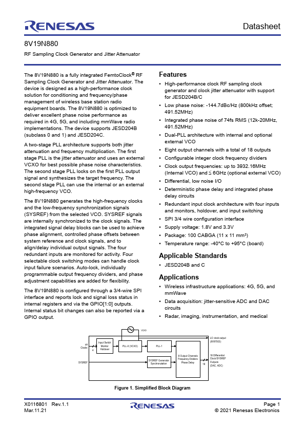
≤4 Clocks
Input Switch Monitor Holdover
SYSREF
VCXO
PLL-0 (VCXO)
PLL-1
SYSREF Generator Synchronziation
LO clock output (8V97003 )
8 Output Channels
18...