• Part: 9DML0441
  • Description: 2:4 3.3V PCIe Gen1-5 Clock Mux
  • Manufacturer: Renesas
  • Size: 628.57 KB
Download 9DML0441 Datasheet PDF
Renesas
9DML0441
9DML0441 is 2:4 3.3V PCIe Gen1-5 Clock Mux manufactured by Renesas.
Description 
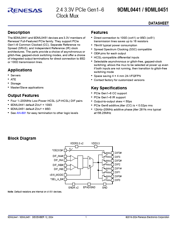
The 9DML0441 and 9DML0451 devices are 3.3V members of Renesas' Full-Featured PCIe family. They support PCIe Gen1- 6 mon Clocked (CC), Separate Reference no Spread (SRn S), and Independent Reference (IR) clock architectures. The parts provide a choice of asynchronous or glitch-free, gapped-clock switching modes, and offer a choice of integrated output terminations for direct connection to 85Ω or 100Ω transmission lines. Applications - Servers - ATE - Storage - Master/Slave applications Output Features - Four 1- 200MHz Low-Power HCSL (LP-HCSL) DIF pairs - 9DML0441 default ZOUT = 100 - 9DML0451 default ZOUT = 85 - See AN-891 for easy termination to other logic levels Features - Direct connection to 100 (xx41) or 85 (xx51) transmission lines saves up to 16 resistors - 79m W typical power consumption - Spread Spectrum Clocking (SSC) patible - OE# pins for each output - HCSL-patible differential inputs - Selectable asynchronous or glitch-free, gapped-clock switching; allows the mux to be selected at power up even if both inputs are not running, then transition to glitch-free switching mode - Space saving 4 × 4 mm 24-VFQFPN - Contact factory for customized versions Key Specifications - PCIe Gen1- 6 CC support - PCIe Gen1- 6 IR support - Output-to-output skew < 50ps - PCIe Gen6 additive jitter (CC) is < 0.02ps rms - 12k Hz- 20MHz additive phase jitter 281fs rms typical at156.25MHz Block Diagram ^OE(3:0)# DIF_INA# DIF_INA DIF_INB# DIF_INB v S W_MO DE ^SE L_A_B # VDDR3.3 x2 4 VDD3.3 Note: Default resistors are internal on 41/51 devices. GNDR x2 EPAD/GND DIF3# DIF3 DIF2# DIF2 DIF1# DIF1 DIF0# DIF0 9DML0441 / 9DML0451 DECEMBER 12, 2024 ©2016-2024 Renesas Electronics...