H7N1005DS
Overview
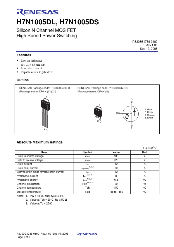
- Low on-resistance RDS (on) = 85 mΩ typ.
- Low drive current
- Capable of 4.5 V gate drive Outline
| Part | H7N1005DS |
|---|---|
| Description | Silicon N-Channel MOS FET |
| Manufacturer | Renesas |
| Size | 113.02 KB |
| Part Number | Manufacturer | Description |
|---|---|---|
| H7N1004LM | Renesas | Silicon N-Channel MOSFET High-Speed Power Switching |
| H7N1004FM | Renesas | Silicon N Channel MOS FET High Speed Power Switching |
| H7N1004FN | Renesas | Silicon N Channel MOS FET High Speed Power Switching |
| H7N1004LS | Renesas | Silicon N-Channel MOSFET High-Speed Power Switching |
| H7N1002LD | Renesas | Silicon N Channel MOS FET High Speed Power Switching |