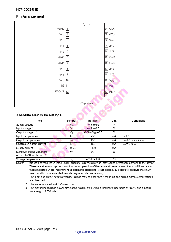
HD74CDC2509B Overview
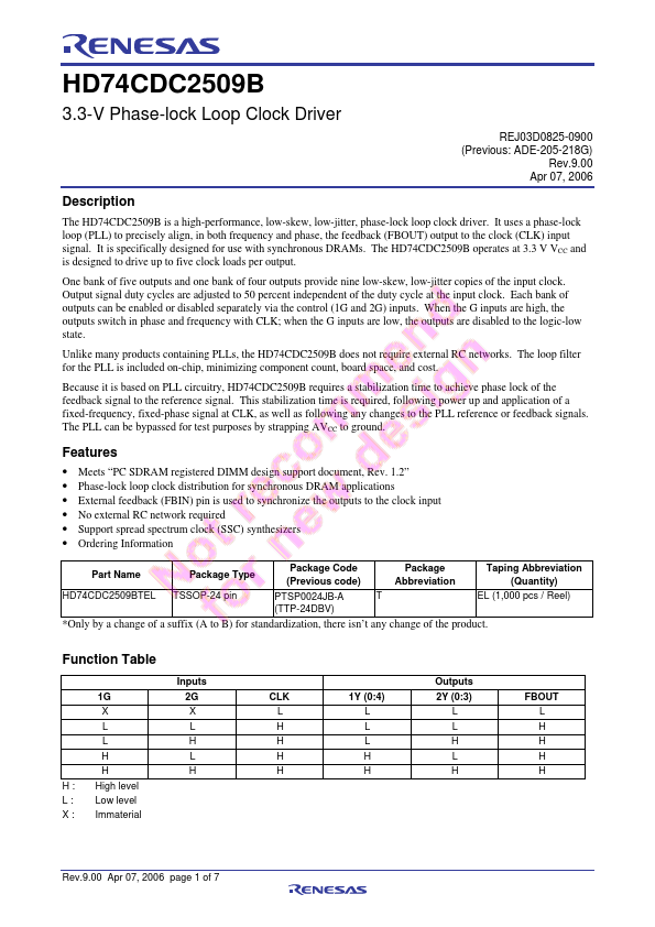
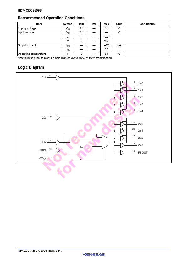
The HD74CDC2509B is a high-performance, low-skew, low-jitter, phase-lock loop clock driver. It uses a phase-lock loop (PLL) to precisely align, in both frequency and phase, the feedback (FBOUT) output to the clock (CLK) input signal. It is specifically designed for use with synchronous DRAMs.