ICS854104
ICS854104 is Differential-to-LVDS Fanout Buffer manufactured by Renesas.
Low Skew, 1-to-4, Differential-to-LVDS Fanout Buffer
General Description
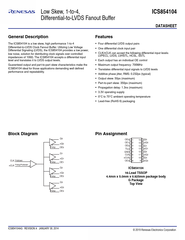
The ICS854104 is a low skew, high performance 1-to-4 Differential-to-LVDS Clock Fanout Buffer. Utilizing Low Voltage Differential Signaling (LVDS), the ICS854104 provides a low power, low noise, solution for distributing clock signals over controlled impedances of 100. The ICS854104 accepts a differential input level and translates it to LVDS output levels.
Guaranteed output and part-to-part skew characteristics make the ICS854104 ideal for those applications demanding well defined performance and repeatability.
Features
- Four differential LVDS output pairs
- One differential clock input pair
-...