Part number:
IDT5V551
Manufacturer:
File Size:
164.61 KB
Description:
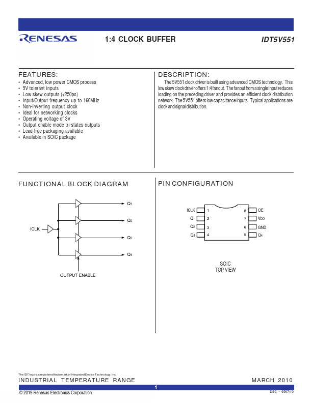
1:4 clock buffer.
IDT5V551 Features
* Advanced, low power CMOS process
* 5V tolerant inputs
* Low skew outputs (
Datasheet Details
IDT5V551
164.61 KB
1:4 clock buffer.
📁 Related Datasheet
IDT5V50009 SPREAD SPECTRUM CLOCK GENERATOR (Renesas)
IDT5V5218 Dual Channel Type-1/Type-2 M-LVDS to LVTTL/LVPECL/LVDS Transceiver (IDT)
IDT5V19EE604 EEPROM PROGRAMMABLE VCXO CLOCK GENERATOR (Renesas)
IDT5V2305 2.5V TO 3.3V HIGH PERFORMANCE CLOCK BUFFER (Integrated Device)
IDT5V2305 HIGH PERFORMANCE CLOCK BUFFER (Renesas)
IDT5V2310 2.5V TO 3.3V HIGH PERFORMANCE CLOCK BUFFER (Integrated Device Technology)
IDT5V2310 HIGH PERFORMANCE CLOCK BUFFER (Renesas)
IDT5V2528 2.5V / 3.3V PHASE-LOCK LOOP CLOCK DRIVER ZERO DELAY BUFFER (Integrated Device)
IDT5V551 Distributor