IDT6V31023
Description
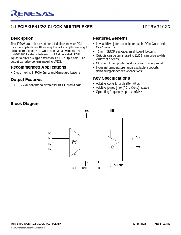
The IDT6V31023 is a 2:1 differential clock mux for PCI Express applications. It has very low additive jitter making it suitable for use in PCIe Gen2 and Gen3 systems.
Key Features
- 1 – 0.7V current mode differential HCSL output pair Features/Benefits
- Low additive jitter; suitable for use in PCIe Gen2 and Gen3 systems
- 16-pin TSSOP package; small board footprint
- Outputs can be terminated to LVDS; can drive a wider variety of devices
- OE control pin; greater system power management
- Industrial temperature range available; supports demanding embedded applications Key Specifications
- Additive cycle-to-cycle jitter <5 ps
- Additive phase jitter (PCIe Gen3) <0.2ps
- Operating frequency up to 200MHz