Datasheet4U Logo Datasheet4U.com

M5M29GB320VP-80 - CMOS Block Erase Flash Memory

Download the M5M29GB320VP-80 datasheet PDF. This datasheet also covers the M5M29GT320VP-80 variant, as both devices belong to the same cmos block erase flash memory family and are provided as variant models within a single manufacturer datasheet.

Description

The Mobile FLASH M5M29GB/T320VP are 3.3V-only high speed 33,554,432-bit CMOS boot block Flash Memories with alternating BGO (Back Ground Operation) feature.

Features

  • Organization 2,097,152 word x 16bit 4,194,304 word x 8 bit Boot Block M5M29GB320VP M5M29GT320VP Bottom Boot Top Boot Supply voltage VCC = 2.7 ~ 3.6V Access time 90ns (Vcc=2.7~3.6V) Power Dissipation 72 mW (Max. at 5MHz) Read (After Automatic Power saving) 0.33µW (typ. ) Program/Erase 126mW (Max. ) 0.33µW (typ. ) Standby Deep power down mode 0.33µW (typ. ) Auto program for Bank(I) and Bank(II) Program Time 4ms (typ. ) Program Unit (Byte Program) 1word/1byte (Page Program) 128word/256by.

📥 Download Datasheet

Note: The manufacturer provides a single datasheet file (M5M29GT320VP-80_Renesas.pdf) that lists specifications for multiple related part numbers.

Full PDF Text Transcription (Reference)

The following content is an automatically extracted verbatim text from the original manufacturer datasheet and is provided for reference purposes only.

View original datasheet text
www.DataSheet4U.com 
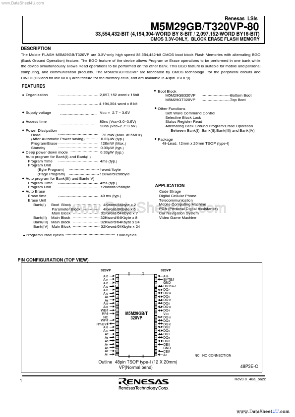
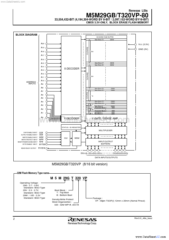
Renesas LSIs 33,554,432-BIT (4,194,304-WORD BY 8-BIT / 2,097,152-WORD BY16-BIT) CMOS 3.3V-ONLY, BLOCK ERASE FLASH MEMORY DESCRIPTION The Mobile FLASH M5M29GB/T320VP are 3.3V-only high speed 33,554,432-bit CMOS boot block Flash Memories with alternating BGO (Back Ground Operation) feature. The BGO feature of the device allows Program or Erase operations to be performed in one bank while the device simultaneously allows Read operations to be performed on the other bank. This BGO feature is suitable for mobile and personal computing, and communication products. The M5M29GB/T320VP are fabricated by CMOS technology for the peripheral circuits and DINOR(Divided bit line NOR) architecture for the memory cells, and are available in 48pin TSOP(I) .
Published: |