Datasheet Summary
..
Renesas LSIs
M6MGB/T32BS8WG
33,554,432-BIT (2,097,152-WORD BY 16-BIT) CMOS FLASH MEMORY 8,388,608-BIT (524,288-WORD BY 16-BIT) CMOS SRAM Stacked-CSP (Chip Scale Package) &
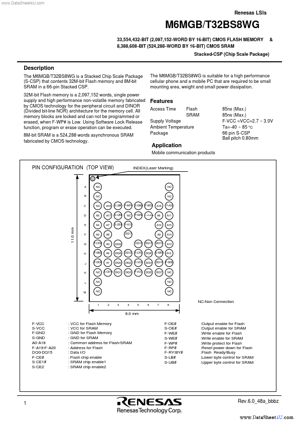
Description
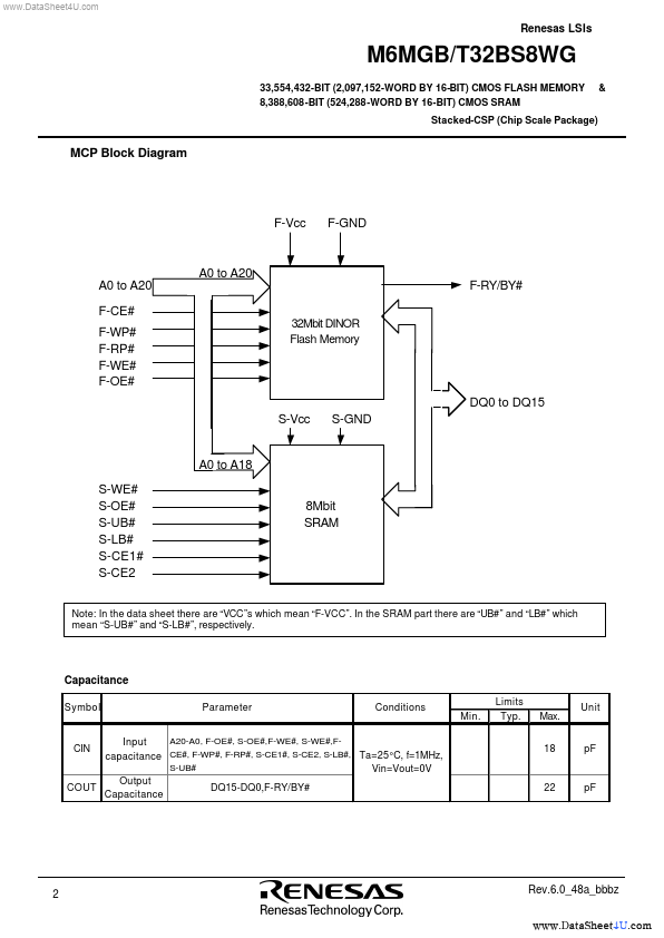
The M6MGB/T32BS8WG is a Stacked Chip Scale Package (S-CSP) that contents 32M-bit Flash memory and 8M-bit SRAM in a 66-pin Stacked CSP. 32M-bit Flash memory is a 2,097,152 words, single power supply and high performance non-volatile memory fabricated by CMOS technology for the peripheral circuit and DINOR (Divided bit-line NOR) architecture for the memory cell. All memory blocks are locked and can not be programmed or erased, when F-WP# is Low. Using Software Lock Release function,...