Datasheet4U Logo Datasheet4U.com

M6MGT33BS8AWG-P - CMOS SRAM

Description

The M6MGB/T33BS8AWG-P is a Stacked Chip Scale Package (S-CSP) that contents 32M-bit Flash memory and 8M-bit SRAM in a 66-pin Stacked CSP with leaded solder ball.

Features

  • Access Time Flash SRAM 70ns (Max. ) 85ns (Max. ) F-VCC =VCC=2.7 ~ 3.0V Ta=-40 ~ 85 °C 66 pin S-CSP Ball pitch 0.80mm Outer-ball:Sn - Pb Supply Voltage Ambient Temperature Package.

📥 Download Datasheet

Full PDF Text Transcription (Reference)

The following content is an automatically extracted verbatim text from the original manufacturer datasheet and is provided for reference purposes only.

View original datasheet text
www.DataSheet4U.com Preliminary Notice: This is not a final specification. Some parametric limits are subject to change. Renesas LSIs M6MGB/T33BS8AWG-P 
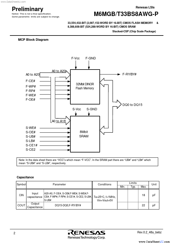
33,554,432-BIT (2,097,152-WORD BY 16-BIT) CMOS FLASH MEMORY 8,388,608-BIT (524,288-WORD BY 16-BIT) CMOS SRAM Stacked-CSP (Chip Scale Package) &
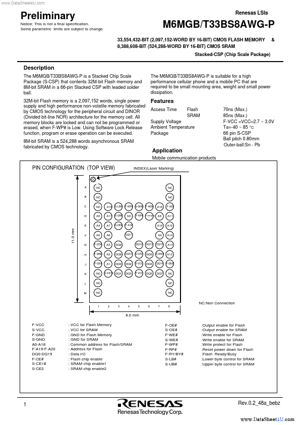
 Description The M6MGB/T33BS8AWG-P is a Stacked Chip Scale Package (S-CSP) that contents 32M-bit Flash memory and 8M-bit SRAM in a 66-pin Stacked CSP with leaded solder ball. 32M-bit Flash memory is a 2,097,152 words, single power supply and high performance non-volatile memory fabricated by CMOS technology for the peripheral circuit and DINOR (Divided bit-line NOR) architecture for the memory cell. All memory blocks are locked and can not be programmed or erased, when F-WP# is Low.
Published: |