M6MGT33BS8BWG Overview
Description
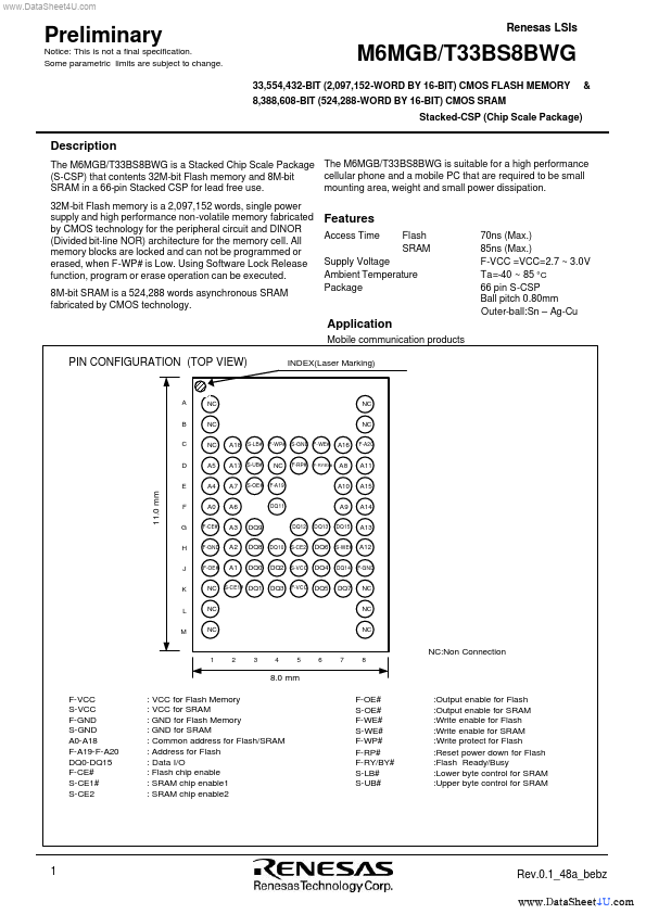
The M6MGB/T33BS8BWG is a Stacked Chip Scale Package The M6MGB/T33BS8BWG is suitable for a high performance cellular phone and a mobile PC that are required to be small (S-CSP) that contents 32M-bit Flash memory and 8M-bit mounting area, weight and small power dissipation. SRAM in a 66-pin Stacked CSP for lead free use.