M6MGT33BS8BWG-P Overview
Description
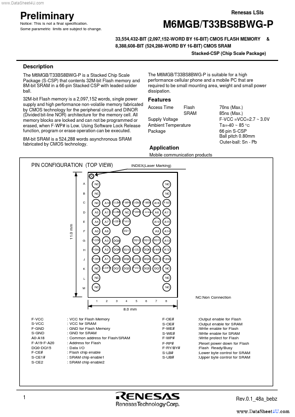
The M6MGB/T33BS8BWG-P is a Stacked Chip Scale Package (S-CSP) that contents 32M-bit Flash memory and 8M-bit SRAM in a 66-pin Stacked CSP with leaded solder ball. 32M-bit Flash memory is a 2,097,152 words, single power supply and high performance non-volatile memory fabricated by CMOS technology for the peripheral circuit and DINOR (Divided bit-line NOR) architecture for the memory cell.
Key Features
- Pb Supply Voltage Ambient Temperature Package