H5N2004DS
H5N2004DS is Silicon N Channel MOS FET High Speed Power Switching manufactured by Renesas.
- Part of the H5N2004DL comparator family.
- Part of the H5N2004DL comparator family.
Features
..
- Low
- Low on-resistance: R DS (on) = 0.38 Ω typ. leakage current: IDSS = 1 µA max (at VDS = 200 V)
- High speed switching: tf = 10 ns typ (at VGS = 10 V, VDD = 100 V, ID = 4 A)
- Low gate charge: Qg = 14 n C typ (at VDD = 160 V, VGS = 10 V, ID = 8 A)
- Avalanche ratings
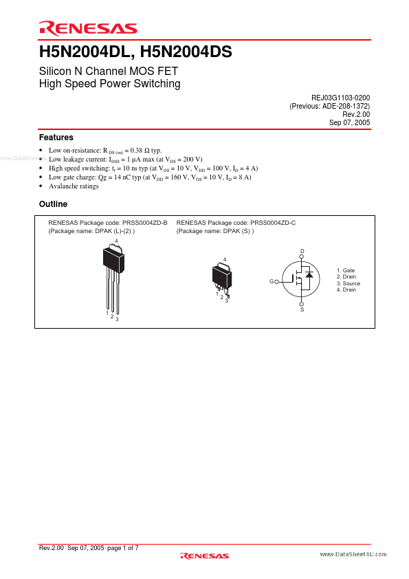
Outline
RENESAS Package code: PRSS0004ZD-B (Package name: DPAK (L)-(2) )
4 D 4 1. Gate 2. Drain 3. Source 4. Drain
RENESAS Package code: PRSS0004ZD-C (Package name: DPAK (S) )
G 1 2
3 S
Rev.2.00 Sep 07, 2005 page 1 of 7
H5N2004DL, H5N2004DS
Absolute Maximum Ratings
(Ta = 25°C)
Item Drain to source voltage Gate to source voltage Drain current Drain peak current Body-drain diode reverse drain current Body-drain diode reverse drain peak current Avalanche current Channel dissipation Channel to case thermal Impedance
.. Channel temperature
Symbol VDSS VGSS ID ID (pulse) IDR
Note 1
Value 200 ±30 8 32 8 32 7 30 4.17 150
- 55 to +150
Unit V V A A A A A W °C/W °C °C
IDR (pulse) Note 3 IAP Pch θ ch-c Tch Tstg
Note 1
Note 2
Storage temperature Notes: 1. PW ≤ 10 µs, duty cycle ≤ 1% 2. Value at Tc = 25°C 3. Tch ≤ 150°C
Electrical Characteristics
(Ta = 25°C)
Item Drain to source breakdown voltage Gate to source leak current Zero gate voltage drain current Gate to source cutoff voltage Static drain to source on state resistance Forward transfer admittance Input capacitance Output capacitance Reverse transfer capacitance Turn-on delay time Rise time Turn-off delay time Fall time Total gate charge Gate to source charge Gate to drain charge Body-drain diode forward voltage Body-drain diode reverse recovery time Body-drain diode reverse recovery charge Note: 4. Pulse test Symbol V (BR) DSS IGSS IDSS VGS (off) RDS (on) |yfs| Ciss Coss Crss td (on) tr td (off) tf Qg Qgs Qgd VDF trr Qrr Min 200
- - 3.0
- 3.3
- -
- -
- -
- -...