The following content is an automatically extracted verbatim text
from the original manufacturer datasheet and is provided for reference purposes only.
View original datasheet text
www.DataSheet4U.com
BLV7002
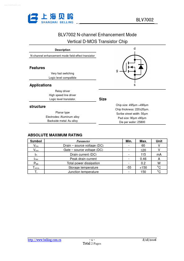
BLV7002 N-channel Enhancement Mode Vertical D-MOS Transistor Chip
Description N-channel enhancement mode field-effect transistor
Features
Very fast switching Logic level compatible
Applications
Relay driver High speed line driver Logic level translator.
Size
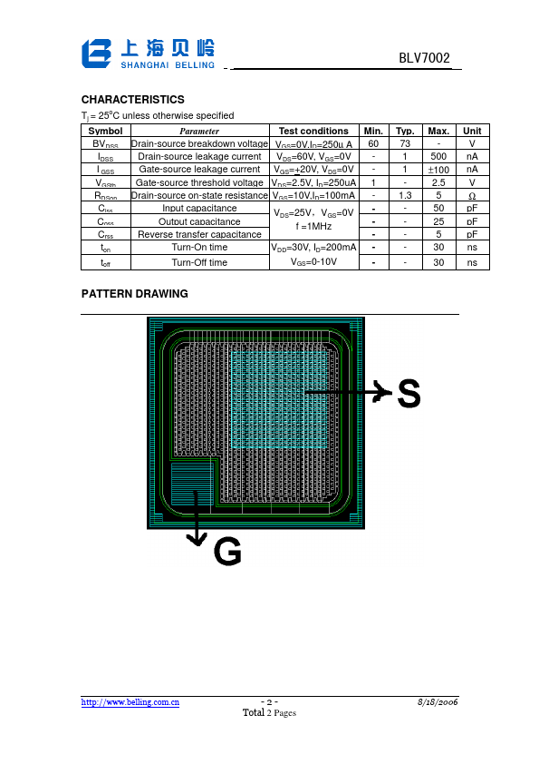
Chip size: 495µm ×490µm Chip thickness: 220±20µm.
structure
Planar type Electrodes: Aluminum alloy Backside metal: Au alloy
Scribe street width: 50µm Pad size: 90µm x90µm Die per wafer: 25800
ABSOLUTE MAXIMUM RATING
Symbol VDS VGS ID IDM Ptot TSTG Tj
Parameter
Drain – source voltage (DC) Gate – source voltage (DC) Drain current (DC) Peak drain current Total power dissipation Storage temperature Junction temperature
Min. -55 -
Max. 60 ±20 115 0.46 0.2 +150 150
Unit V V mA A W o C o C
http://www.