STF10NM65N Overview
Description
This series of devices implements the second generation of MDmesh™ Technology. This revolutionary Power MOSFET associates a new vertical structure to the Company’s strip layout to yield one of the world’s lowest on-resistance and gate charge.
Key Features
- Limited only by maximum temperature allowed
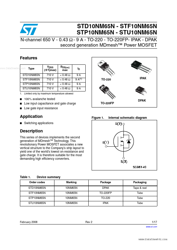
- 3 1 3 1 2 100% avalanche tested Low input capacitance and gate charge Low gate input resistance Figure
- TO-220FP DPAK