STU6NA90
STU6NA90 is N-channel Power MOSFET manufactured by STMicroelectronics.
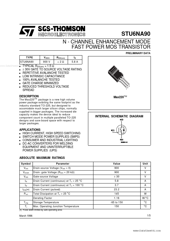
DESCRIPTION
Max220TM
INTERNAL SCHEMATIC DIAGRAM
APPLICATIONS s HIGH CURRENT, HIGH SPEED SWITCHING s SWITCH MODE POWER SUPPLIES (SMPS) s CONSUMER AND INDUSTRIAL LIGHTING s DC-AC CONVERTERS FOR WELDING EQUIPMENT AND UNINTERRUPTIBLE POWER SUPPLIES (UPS) ABSOLUTE MAXIMUM RATINGS
Symbol V DS VDGR V GS ID ID I DM (
- ) P tot T stg Tj Parameter Drain-source Voltage (V GS = 0) Drain- gate Voltage (R GS = 20 k Ω ) Gate-source Voltage Drain Current (continuous) at T c = 25 o C Drain Current (continuous) at T c = 100 o C Drain Current (pulsed) Total Dissipation at T c = 25 C Derating Factor Storage Temperature Max. Operating Junction Temperature o
Value 900 900 ± 30 5.8 3.7 23.2 145 1.16 -65 to 150 150
Unit V V V A A A W W/ o C o o
(- ) Pulse width limited by safe operating area
March 1996
1/5
THERMAL DATA
R thj-case
Rthj-amb
R thc-sink TI
Thermal Resistance Junction-case Thermal Resistance Junction-ambient Thermal Resistance Case-sink Maximum Lead Temperature For Soldering Purpose
Max Max Typ
0.86 30 0.1 300 o o
C/W C/W o C/W o C
AVALANCHE CHARACTERISTICS
Symbol I AR
..
Parameter Avalanche Current, Repetitive or Not-Repetitive (pulse width limited by T j max, δ < 1%) Single Pulse Avalanche Energy (starting T j = 25 o C, ID = I AR , V DD = 50 V) Repetitive Avalanche Energy (pulse width limited by T j max, δ < 1%) Avalanche Current, Repetitive or Not-Repetitive (T c = 100 o C, pulse width limited by T j max, δ < 1%)
Max Value 6 180 7.2 3.8
Unit A m J m J A
E AS EAR I AR
ELECTRICAL CHARACTERISTICS (Tcase = 25 o C unless otherwise specified) OFF
Symbol V (BR)DSS I DSS I GSS Parameter Drain-source Breakdown Voltage Test Conditions I D = 250 µ A VGS = 0 Min. 900 250 1000 ± 100 Typ. Max. Unit V µA µA n A
Zero Gate Voltage V DS = Max Rating Drain Current (V GS = 0) V DS = Max Rating x 0.8 Gate-body Leakage Current (V DS = 0) V GS = ± 30 V
T c = 125 o C
ON (∗)
Symbol V GS(th) R DS(on) ID(on) Parameter Gate Threshold Voltage V DS = VGS Static...