K4D551638H-LC40 Description
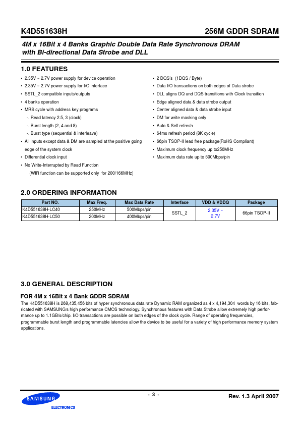
FOR 4M x 16Bit x 4 Bank GDDR SDRAM.
K4D551638H-LC40 Key Features
- 2.35V ~ 2.7V power supply for device operation
- 2.35V ~ 2.7V power supply for I/O interface
- SSTL_2 patible inputs/outputs
- 4 banks operation
- MRS cycle with address key programs
- Read latency 2.5, 3 (clock) -. Burst length (2, 4 and 8) -. Burst type (sequential & interleave)
- All inputs except data & DM are sampled at the positive going edge of the system clock
- Differential clock input
- No Write-Interrupted by Read Function
- 2 DQS’s (1DQS / Byte)
K4D551638H-LC40 Applications
- Samsung Electronics reserves the right to change products or specification without notice