K7P401822B Description
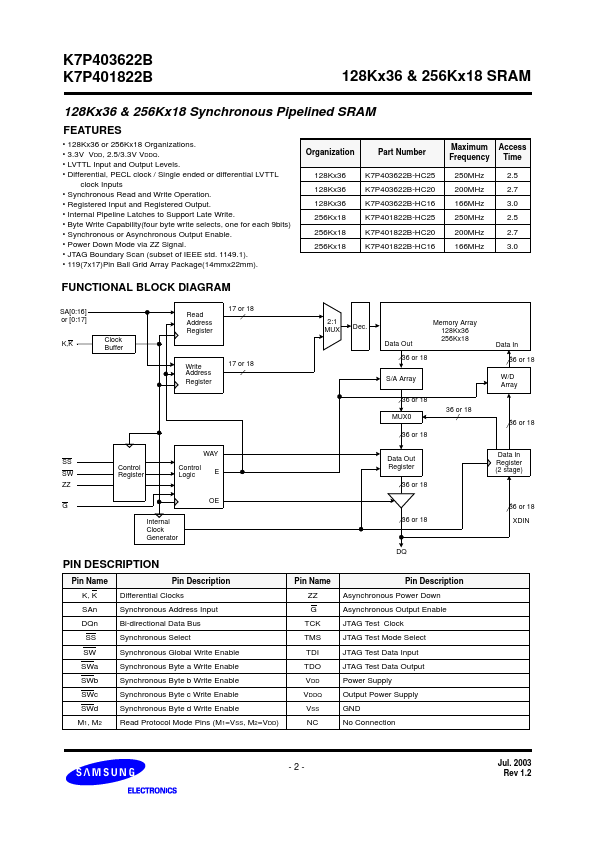
Pin Name K, K SAn DQn SS SW SWa SWb SWc SWd M1, M2 Pin Description Differential Clocks Synchronous Address Input Bi-directional Data Bus Synchronous Select Synchronous Global Write Enable Synchronous Byte a Write Enable Synchronous Byte b Write Enable Synchronous Byte c Write Enable Synchronous Byte d Write Enable Read Protocol Mode Pins (M1=VSS, M2=VDD) Data Out Register 36 or 18 36 or 18 DQ Pin Name ZZ G TCK TMS...
K7P401822B Key Features
- 128Kx36 or 256Kx18 Organizations
- 3.3V VDD, 2.5/3.3V VDDQ
- LVTTL Input and Output Levels
- Differential, PECL clock / Single ended or differential LVTTL
- Synchronous Read and Write Operation
- Registered Input and Registered Output
- Internal Pipeline Latches to Support Late Write
- Byte Write Capability(four byte write selects, one for each 9bits)
- Synchronous or Asynchronous Output Enable
- Power Down Mode via ZZ Signal