• Part: K6R1008V1D
  • Description: 64Kx16 Bit High-Speed CMOS Static RAM(3.3V Operating) Operated at Commercial and Industrial Temperature Ranges.
  • Manufacturer: Samsung Semiconductor
  • Size: 181.85 KB
Download K6R1008V1D Datasheet PDF
Samsung Semiconductor
K6R1008V1D
K6R1008V1D is 64Kx16 Bit High-Speed CMOS Static RAM(3.3V Operating) Operated at Commercial and Industrial Temperature Ranges. manufactured by Samsung Semiconductor.
FEATURES - 
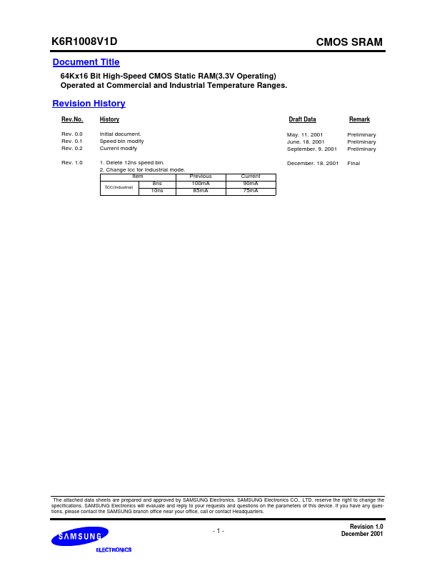
Fast Access Time 8,10ns(Max.) - Low Power Dissipation Standby (TTL) : 20m A(Max.) (CMOS) : 5m A(Max.) Operating K6R1008V1D-08: 80m A(Max.) K6R1008V1D-10: 65m A(Max.) - Single 3.3±0.3V Power Supply - TTL patible Inputs and Outputs - Fully Static Operation - No Clock or Refresh required - Three State Outputs - Center Power/Ground Pin Configuration - Standard Pin Configuration K6R1008V1D-J : 32-SOJ-400 K6R1008V1D-T : 32-TSOP2-400CF - Operating in mercial and Industrial Temperature range. for AT&T CMOS SRAM GENERAL DESCRIPTION The K6R1008V1D is a 1,048,576-bit high-speed Static Random Access Memory organized as 131,072 words by 8 bits. The K6R1008V1D uses 8 mon input and output lines and has an output enable pin which operates faster than address access time at read cycle. The device is fabricated using SAMSUNG ′s advanced CMOS process and designed for high-speed circuit technology. It is particularly well suited for use in high-density high-speed system applications. The K6R1008V1D is packaged in a 400mil 32-pin plastic SOJ or TSOP2 forward. 128K x 8 Bit High-Speed CMOS Static RAM(3.3V Operating) PIN CONFIGURATION(Top View) A0 A1 A2 A3 CS I/O1 I/O2 1 2 3 4 5 6 7 8 9 32 A16 31 A15 30 A14 29 A13 28 OE 27 I/O8 26 I/O7 FUNCTIONAL BLOCK DIAGRAM Vcc Vss SOJ/ TSOP2 25 Vss 24 Vcc 23 I/O6 22 I/O5 21 A12 20 A11 19 A10 18 17 A9 A8 I/O3 10 Clk Gen. A0 A1 A2 A3 A4 A5 A6 A7 A8 Pre-Charge Circuit I/O4 11 WE A4...