2SA648
2SA648 is Silicon POwer Transistors manufactured by SavantIC.
SavantIC Semiconductor
..
Product Specification
Silicon PNP Power Transistors
DESCRIPTION
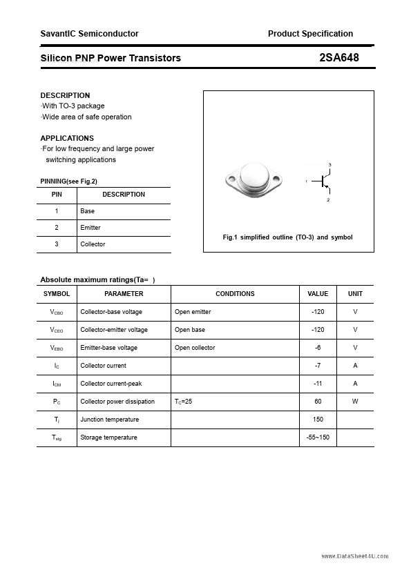
- With TO-3 package
- Wide area of safe operation APPLICATIONS
- For low frequency and large power switching applications
PINNING(see Fig.2) PIN 1 2 3 Base Emitter Fig.1 simplified outline (TO-3) and symbol Collector...