2SB552
Description
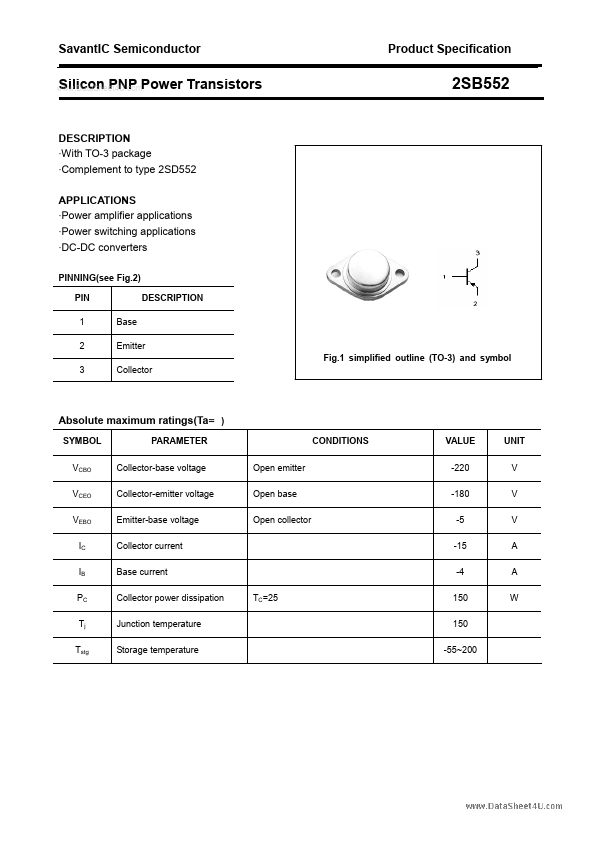
With TO-3 package - plement to type 2SD552 APPLICATIONS - Power amplifier applications - Power switching applications - DC-DC converters PINNING(see Fig.2) PIN 1 2 3 Base Emitter Fig.1 simplified outline (TO-3) and symbol Collector DESCRIPTION SYMBOL VCBO VCEO VEBO IC IB PC Tj Tstg PARAMETER Collector-base voltage Collector-emitter voltage Emitter-base voltage Collector current Base current Collector power dissipation Junction temperature Storage temperature TC=25 Open emitter Open base Open collector CONDITIONS VALUE -220 -180 -5 -15 -4 150 150 -55~200 UNIT V V V A A W SavantIC Semiconductor.