SI53301
SI53301 is 1:6 LOW JITTER UNIVERSAL BUFFER/LEVEL TRANSLATOR manufactured by Silicon Labs.
Features
- 6 differential or 12 LVCMOS outputs
- Loss of signal (LOS) monitors for
- Ultra-low additive jitter: 45 fs rms loss of input clock
- Wide frequency range: 1 to 725 MHz
- Independent VDD and VDDO :
- Universal any-format input with pin
1.8/2.5/3.3 V selectable output formats
- 1.2/1.5 V LVCMOS output support
- LVPECL, low power LVPECL, LVDS,
- Selectable LVCMOS drive strength to
CML, HCSL, LVCMOS tailor jitter and EMI performance
- 2:1 input mux
- Small size: 32-QFN (5 mm x 5 mm)
- Glitchless input clock switching
- Ro HS pliant, Pb-free
- Synchronous output enable
- Industrial temperature range:
- Output clock division: /1, /2, /4
- 40 to +85 °C
Applications
- High-speed clock distribution
- Ethernet switch/router
- Optical Transport Network (OTN)
- SONET/SDH
- PCI Express Gen 1/2/3
- Storage
- Tele
- Industrial
- Servers
- Backplane clock distribution
Description
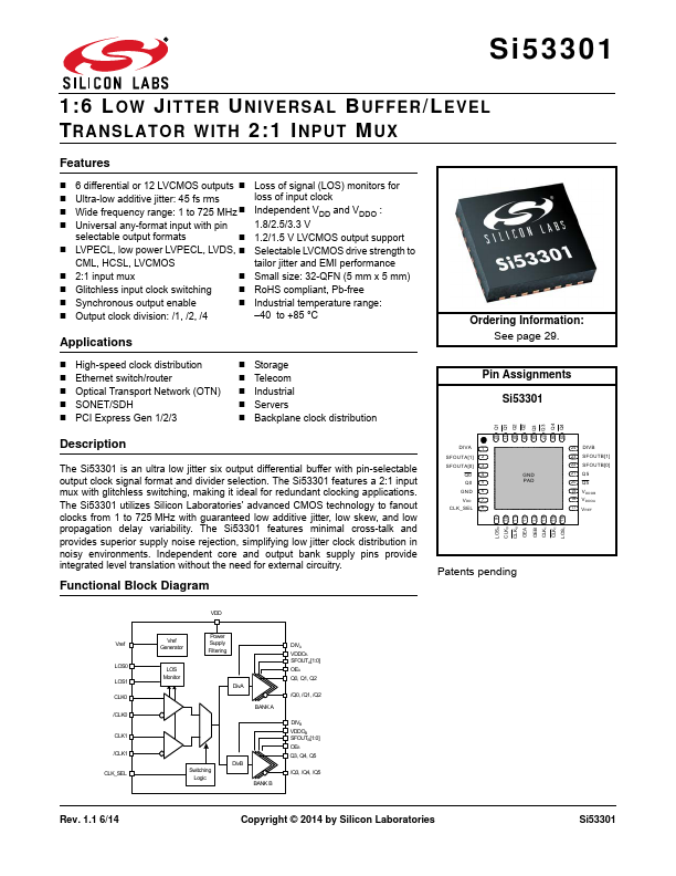
The Si53301 is an ultra low jitter six output differential buffer with pin-selectable output clock signal format and divider selection. The Si53301 features a 2:1 input mux with glitchless switching, making it ideal for redundant clocking applications. The Si53301 utilizes Silicon Laboratories' advanced CMOS technology to fanout clocks from 1 to 725 MHz with guaranteed low additive jitter, low skew, and low propagation delay variability. The Si53301 features minimal cross-talk and provides superior supply noise rejection, simplifying low jitter clock distribution in noisy environments. Independent core and output bank supply pins provide integrated level translation without the need for external circuitry.
Functional Block Diagram
Ordering Information: See page 29.
Pin Assignments Si53301
25 26 27 28 29 30 31 32
DIVA
SFOUTA[1] SFOUTA[0]
Q0 Q0 GND VDD...