SI53303
SI53303 is DUAL 1:5 LOW JITTER BUFFER/LEVEL TRANSLATOR manufactured by Silicon Labs.
Features
- 10 differential or 20 LVCMOS outputs- Independent VDD and VDDO :
- Ultra-low additive jitter: 100 fs rms
1.8/2.5/3.3 V
- Wide frequency range: 1 to 725 MHz- Excellent power supply noise
- Any-format input with pin selectable rejection (PSRR) output formats: LVPECL, Low Power
- Selectable LVCMOS drive strength to
LVPECL, LVDS, CML, HCSL, tailor jitter and EMI performance
LVCMOS
- Small size: 44-QFN (7 mm x 7 mm)
- Synchronous output enable
- Ro HS pliant, Pb-free
- Output clock division: /1, /2, /4
- Industrial temperature range:
- Low output-output skew: <50 ps
- 40 to +85 °C
- Low propagation delay variation:
<400 ps
Applications
- High-speed clock distribution
- Ethernet switch/router
- Optical Transport Network (OTN)
- SONET/SDH
- PCI Express Gen 1/2/3
- Storage
- Tele
- Industrial
- Servers
- Backplane clock distribution
Description
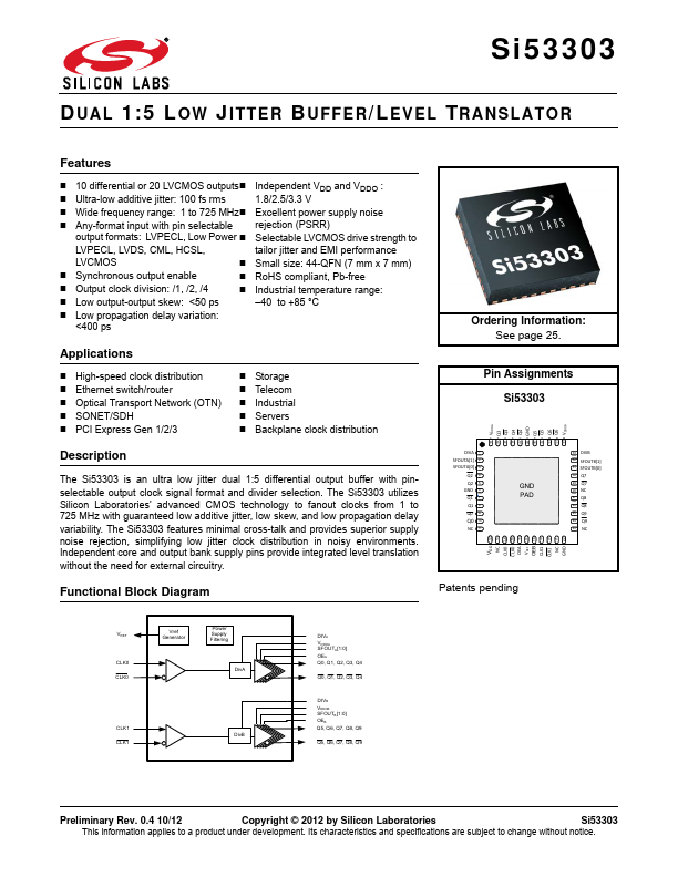
The Si53303 is an ultra low jitter dual 1:5 differential output buffer with pinselectable output clock signal format and divider selection. The Si53303 utilizes Silicon Laboratories' advanced CMOS technology to fanout clocks from 1 to 725 MHz with guaranteed low additive jitter, low skew, and low propagation delay variability. The Si53303 features minimal cross-talk and provides superior supply noise rejection, simplifying low jitter clock distribution in noisy environments. Independent core and output bank supply pins provide integrated level translation without the need for external circuitry.
Functional Block Diagram
Ordering Information: See page 25.
Pin Assignments Si53303
VDDOA Q3 Q3 Q4 Q4 GND Q5 Q5 Q6 Q6 VDDOB
34 35 36 37 38 39 40 41 42 43 44
DIVA 1
SFOUTA[1] 2 SFOUTA[0] 3
Q2 Q2 GND Q1
4 5 6...