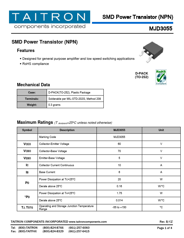
MJD3055 Description
(800)-TAITRON (800)-824-8766 (661)-257-6060 Fax: (800)-TAITFAX (800)-824-8329 (661)-257-6415 Unit V V V A A W W/°C W W/°C °C Rev.
MJD3055 Key Features
- Designed for general purpose amplifier and low speed switching
MJD3055 is SMD Power Transistor manufactured by Taitron Components.
| Manufacturer | Part Number | Description |
|---|---|---|
| MJD3055 | Silicon NPN Power Transistor | |
| MJD3055 | General Purpose Amplifier | |
| MJD3055 | Complementary Silicon Power Transistors | |
| MJD3055 | Complementary Power Transistors | |
| MJD3055 | SILICON POWER TRANSISTORS |
(800)-TAITRON (800)-824-8766 (661)-257-6060 Fax: (800)-TAITFAX (800)-824-8329 (661)-257-6415 Unit V V V A A W W/°C W W/°C °C Rev.